
 ON Semiconductor has announced its X-Class image sensor platform, which allows a single camera design to support not only multiple product resolutions but also different pixel functionality. The first devices in the new platform are the 12 megapixel (MP) XGS 12000 and 4k / UHD resolution XGS 8000 image sensors, which provide high-performance imaging capabilities for applications such as machine vision, intelligent transportation systems, and broadcast imaging.
The X-Class image sensor platform enables a new dimension in camera design by supporting multiple CMOS pixel architectures within the same image sensor frame. This allows a single camera design not only to support multiple product resolutions, but also different pixel functionality, such as larger pixels that trade resolution at a given optical format for higher imaging sensitivity, designs optimized for low noise operation to increase dynamic range, and more. By supporting these different pixel architectures through a common high bandwidth, low power interface, camera manufacturers can leverage existing parts inventory and accelerate time to market for new camera designs.
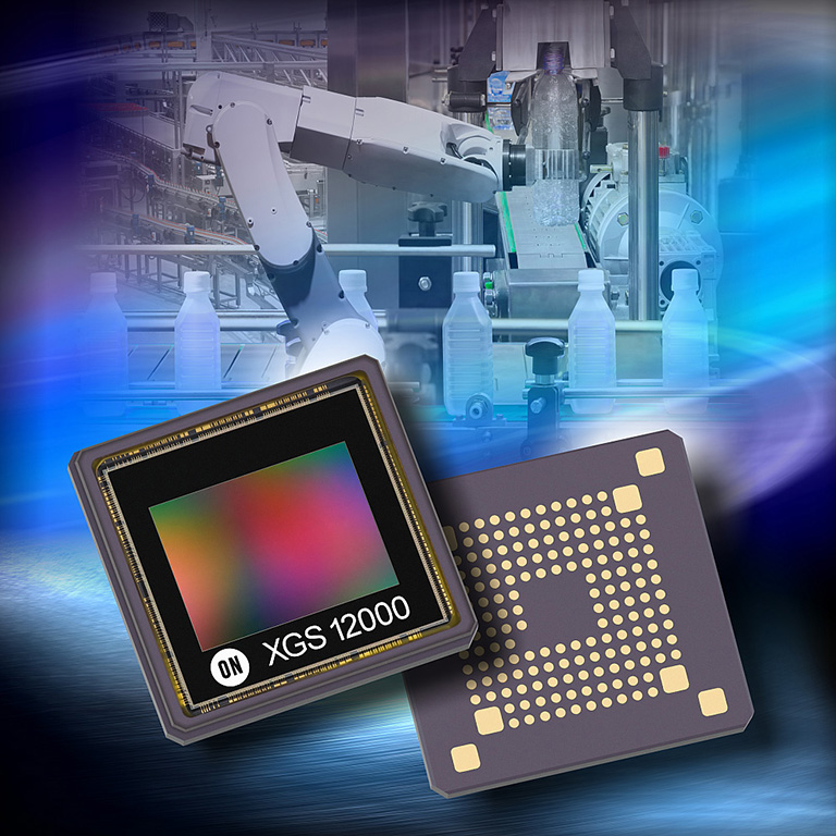
The initial devices in the X-Class family, the XGS 12000 and XGS 8000, are based on the first pixel architecture to be deployed in this platform – an advanced 3.2 µm global shutter CMOS pixel that features superior imaging performance, high image uniformity, and low noise. The XGS 12000 provides 12 MP (4096 x 3072 pixel) resolution in a one-inch optical format to supply the imaging detail and performance needed for modern machine vision and inspection applications. The device is planned to be available in two speed grades – one that fully utilizes 10GigE interfaces by providing full resolution speeds up to 90 frames per second (fps), and a lower price version providing 27 fps at full resolution that aligns with the bandwidth available from USB 3.0 computer interfaces. The XGS 8000 provides 4k / UHD (4096 x 2160 pixels) resolution in a 1/1.1 inch optical format and is also planned to be available in two speed grades (130 and 75 fps), making the device ideal for broadcast applications.
The package dimensions of both devices combine with a low thermal profile enabled by the low-voltage, low-power architecture of the X-Class interface to make them fully compatible with compact 29 x 29 mm2 camera designs.
The XGS 12000 and XGS 8000
Leave a Reply