A new kind of flash memory is optimized specifically to handle the hostile environment imposed on electronics in vehicular uses.
Leland Teschler | Executive Editor
You’d have to say the NAND flash memory had an inauspicious beginning. Invented in 1987 by Toshiba, the first NAND flash chip didn’t sell until 1995 when it finally found a spot in digital answering machines. Toshiba insiders say the company almost killed the project twice. When the technology finally made a commercial debut, it was in the form of a 4-Mbit part that went for a mere $10 per megabit.
Today, the same die area that held a 4-Mbit flash part in 1995 can hold 1.33 trillion bits, a factor of 333,000-times denser than the first part. And the price has dropped to two-hundredths of a cent per megabit, or about 20 cents per gigabit. Meanwhile, the NAND flash market has grown to something north of $60 billion as of last year thanks largely to applications ranging from digital cameras to cellphones. Meanwhile, industry analysts figure the NAND flash market is growing at a rate of about 40% annually and will continue to do so thanks to demand in uses such as data centers, servers, smartphones, tablets, and PCs.

Interestingly, uses in connected vehicles don’t constitute much of the projected demand – yet. That’s about to change with the rise of ADAS technology and autonomous piloting functions. Analysts figure the average autonomous vehicle will generate data at the rate of 4 terabytes per day, and a lot of that data will be uploaded to the cloud. Much of it will necessarily sit in flash memory chips residing both on vehicles and in data centers. The upshot of these trends is a boom time for flash chips that can handle the special needs of vehicles.
Going for a ride
Automakers are notorious for their penny pinching on components. In the case of flash memory, they have an advantage in the cost area: smartphones are one of the biggest uses for flash chips, and there some 1.5 billion smartphones sold annually. Memory suppliers say that huge volume can help them keep down costs of flash chip destined for automotive use because there are a lot of commonalities between the memory chips deployed in both applications.
Today, the main flash memory used in vehicles follows a Jedec (Joint Electron Device Engineering Council) standard called e-MMC, short for embedded Multi-Media Controller. It simply refers to a package consisting of both flash memory and a flash memory controller integrated on the same silicon die. This format has been the mainstay flash memory for mid to high-end cell phones.
But the e-MMC format is showing its age. The main problem is that e-MMC employs and eight-bit parallel interface. This type of connection has a limited interface speed that can’t match the demanding mobile and mobile-influenced applications now coming down the pike.
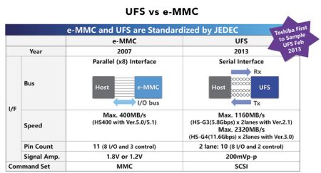
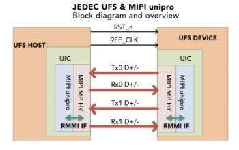
The Universal Flash Storage (UFS) Jedec format is designed to remedy problems with e-MMC. A key difference is that UFS uses a serial differential-signaling serial interface rather than a parallel interface.
Additionally, the parallel eight-bit interface of eMMC forced read and write operations to be sequential, or half-duplex. The new UFS standard has dedicated read and write paths to permit simultaneous reads and writes. The serial interface and full-duplex data transfers let UFS realize two to four times the peak bandwidth of eMMC and do so with more power efficiency. The peak bandwidth of UFS defined so far reaches 11.6 Gbps over two lanes.
UFS also incorporates a feature called Command Queue (CQ), similar to that of recent e-MMC memories, which makes use of the multitasking features of mobile operating systems and multi-core CPUs. This feature allows the parallel execution of multiple read and write commands, significantly boosting command processing speeds.
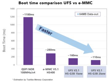
These improvements allow the latest version of the UFS standard to boost sequential read speeds by 40%, sequential write speeds by 20%, and the number of input/output operations per second for random reads by 73% compared to what’s possible with e-MMC devices. Overall, UFS improves system boot times by 15% and application loading times by 30% compared to that of e-MMC.
And UFS incorporates features that are particularly useful in automotive settings. Among them are thermal control where a UFS device exceeding 105°C notifies the host processor so it can take corrective action. Thanks to a feature called extended diagnosis, the UFS controller monitors operational parameters such as read/write cycles and temperature, then reports its status to the host processor.
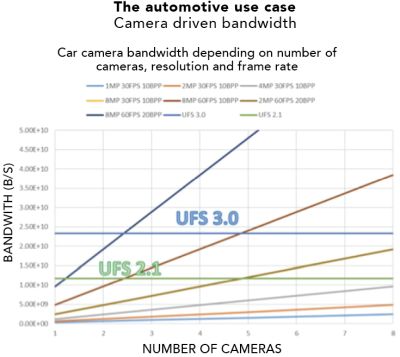
Industry analysts also say automotive uses impose demands on flash chips that other consumer applications don’t. Perhaps the most obvious of these is an extended temperature range, but flash suppliers will likely field versions of their products with other qualifications necessary for automotive use. These qualifications include adherence to a PPAP (Production Part Approval Process), an industry guideline detailing the specific reports and documentation necessary to gain part approval in the automotive industry. And because vehicles have a much longer expected life than other consumer products, flash suppliers expect to provide lengthy periods of support and longer-than-usual product change notifications (PCNs).
All in all, UFS is starting to migrate from high-end phones to mainstream mobile markets, and in the near future will find a prominent spot in automotive applications.






Leave a Reply