
Samsung researchers have advanced the concept of a solid-state lidar with the development of a single-chip device with a 10-m range.
Light Detection and Ranging (lidar) technology normally requires flash illumination or beam scanning to detect surroundings. The problem is such schemes generally demand use of a high-power laser. So most commercially available long-range lidar units employ mechanical beam scanners with rotating motors and mirrors. Solid-state versions of lidar avoid some of the problems with mechanical versions, but they still use separate lasers to get the kind of detection ranges that are practical for commercial use.
Researchers from Samsung say they have been able to integrate all the major lidar components onto a single chip. Specifically, the chip holds optical phased arrays (OPA), an integrated tunable laser diode (TLD), and semiconductor optical amplifiers (SOAs). An ultrafast, self-evolving genetic OPA-calibration algorithm and digital signal processing manages the device.
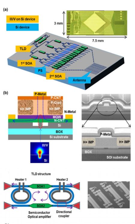
Illustration and microscope image of fully-integrated 32-channel scanner. The chip size is 7.5×3.0 mm. (b) Illustration and vertical SEM image of III/V on Si device (TLD and SOA). Below, illustration and SEM image of TLD structure.
Scheduled to present at the upcoming IEDM conference (Paper 7.2, “Single-Chip Beam Scanner with Integrated Light Source for Real-Time Light Detection and Ranging,” J. Lee et al, Samsung), the group says the chip works at a wavelength of 1.3 μm and has a resolution of 120 (horizontal) × 20 (vertical) lines, a scan range up to 10 m, a scan speed of 20 fps, a small beam divergence of 0.15°×0.09°, and a field of view (FOV) of 15°×3.5°.
Light from the laser diode is divided into 32 channels through cascaded beam splitters, and the 32 optical phases are adjusted by a phase shifter at each channel. A set of optical amplifiers (four in the first stage. 32 in the second stage) amplify the laser light. Finally an optical beam is emitted from a grating-based antenna array. The horizontal and vertical directions of the output beam are controlled by optical phase control and wavelength control respectively.
Besides the laser diode, optical amps and phased arrays, the scanner chip also contains various silicon photonics devices waveguides, multimode interference (MMI) splitters, p-i-n phase shifters (PSs), and
an optical antenna array with an aperiodic design. The chip was fabricated on a silicon-on-insulator (SOI) wafer. For the TLD and SOAs requiring optical gain, III-V epitaxial layers were directly bonded to the pre-patterned silicon wafer and post-processed to form the photonic circuit.
The laser diode is a Vernier ring laser composed of two ring resonators and two SOAs. A ring laser contains a set of waveguides in which at least one is a closed loop coupled to a light input and output. When light of the resonant wavelength passes through the loop from input waveguide, it builds up in intensity over multiple round-trips due to constructive interference and is output to the output bus waveguide which serves as a detector waveguide. Only a select few wavelengths will be at resonance within the loop, so the optical ring resonator functions as a filter. Both rings are designed to have slightly different circumferences for a selective resonance of a single longitudinal mode through the Vernier effect. The laser wavelength is then tuned by the heaters in the ring resonators.
Researchers measured time-of-flight (TOF) and quality of signal (QOS) of the received pulses and reconstructed them in a viewer to create 3-D depth images and point clouds. Gathering TOFs and QOSs with 20 pulse accumulation over 120×20 pixels, researchers could get one depth image within 0.048 sec, leading to over 20 frames per second. To figure range accuracy and precision, researchers measured averages and standard deviations of range over the distance to a white flat reference wall. The range errors were smaller than ~10cm. Range fluctuations corresponding to precision were less than 8 cm from 1 to 10 m.
The 66th annual edition of the IEEE International Electron Devices Meeting (IEDM), the world’s premier forum for the presentation of applied research in transistors and related devices, will take place virtually this year. The conference will now run from Saturday through Friday, December 12-18, 2020, and will offer a mix of live-streamed events and on-demand pre-recorded presentations, with a schedule of live Q&A sessions. The expanded schedule is intended to give global attendees enough time to review the more than 220 papers in the IEDM technical program, plus the tutorials and short courses, and to participate in the live-streamed events, such as the plenary presentations, panel discussion and career session.
This year’s theme is “Innovative Devices for a Better Future,” which reflects the fact that, at a time of great global uncertainty, electronics technology is being used much more broadly than ever before to address the world’s most pressing challenges.
“This year’s format may be different, but what hasn’t changed at all is that IEDM will once again offer an outstanding technical program that showcases important breakthroughs in key semiconductor and related technologies, which are essential for the progress of modern society,” said Dina Triyoso, IEDM 2020 Publicity Chair and Technologist at TEL Technology Center, America, LLC. “I’m very proud of the fact that, despite the laboratory restrictions and all of the other challenges imposed on us by the pandemic, our community has persevered and driven the state-of-the-art of electronics technology forward yet again.”
“Although a virtual experience doesn’t give us the ability to see our colleagues in person, it does provide unique opportunities which we have tried to maximize,” said Meng-Fan (Marvin) Chang, IEDM 2020 Publicity Vice Chair, IEEE Fellow, Distinguished Professor of Electrical Engineering at National Tsing Hua University and Director of Corporate Research at TSMC. “For example, if IEDM were a physical event this year, nine technical sessions would run in parallel. An attendee likely would find it difficult to attend all talks of interest. But with recorded presentations available on-demand a week ahead of time, that roadblock is eliminated.”


Leave a Reply