• Skip to primary navigation
  • Skip to main content
  • Skip to primary sidebar
  • Skip to footer

Microcontroller Tips

Microcontroller engineering resources, new microcontroller products and electronics engineering news

  • Products
    • 8-bit
    • 16-bit
    • 32-bit
    • 64-bit
  • Applications
    • 5G
    • Automotive
    • Connectivity
    • Consumer Electronics
    • EV Engineering
    • Industrial
    • IoT
    • Medical
    • Security
    • Telecommunications
    • Wearables
    • Wireless
  • Learn
    • eBooks / Tech Tips
    • EE Training Days
    • FAQs
    • Learning Center
    • Tech Toolboxes
    • Webinars/Digital Events
  • Resources
    • Design Guide Library
    • DesignFast
    • LEAP Awards
    • Podcasts
    • White Papers
  • Videos
    • EE Videos & Interviews
    • Teardown Videos
  • EE Forums
    • EDABoard.com
    • Electro-Tech-Online.com
  • Engineering Training Days
  • Advertise
  • Subscribe

50 Mp CCD image sensor targets inspection of smartphone displays

October 30, 2018 By Aimee Kalnoskas Leave a Comment

ON Semiconductor is enabling more efficient inspection of smartphone displays with the introduction of a new 50 megapixel (MP) resolution charge-coupled device (CCD) image sensor. As the highest resolution KAI-50140 50 Mp CCD image sensor 
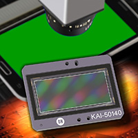
Transfer CCD image sensor commercially available, the KAI-50140 provides the critical imaging detail and high image uniformity needed not only for inspection of smartphone displays but also circuit board and mechanical assembly inspection as well as aerial surveillance.

The KAI-50140 is designed in a 2.18 to 1 aspect ratio to match the format of modern smartphones, reducing the number of image captures required to inspect a full display. The 4.5 µm Interline Transfer CCD pixel used in the KAI-50140 provides high resolution with a true electronic (global) shutter while preserving critical imaging performance. The new device supports frame rates up to 4 fps through the use of flexible 1, 2, or 4 output readout architecture, and shares the same pin definitions as both the popular 29 MP KAI-29050 and KAI-29052 as well as the KAI-43140 image sensors. This allows the KAI-50140 to be incorporated into existing camera designs with only minor electrical changes – speeding time-to-market for adoption of the new device.

“As the specifications and aspect ratios of smartphone displays continue to expand in both physical size as well as pixel density, we were compelled to develop an image sensor designed specifically for inspection of these devices,” said Herb Erhardt, Vice President and General Manager, Industrial Solutions Division, Intelligent Sensing Group at ON Semiconductor. “The unique combination of high resolution, unmatched image uniformity, and 2.18:1 pixel arrangement provided by the KAI-50140 enables higher quality, more efficient inspection of modern smartphone displays.”

The KAI-50140 is sampling today with production planned by the end of 2018, and is available in a ceramic PGA package in both monochrome and Bayer Color configurations. The KAI-50140 will be demonstrated as part of ON Semiconductor’s exhibit in booth 1B32 at the VISION 2018 trade fair, held Nov 6 – 8 2018 in Stuttgart, Germany.

Filed Under: Applications, Consumer Electronics, Security Tagged With: onsemiconductor

Reader Interactions

Leave a Reply Cancel reply

Your email address will not be published. Required fields are marked *

Primary Sidebar

Featured Contributions

Five challenges for developing next-generation ADAS and autonomous vehicles

Securing IoT devices against quantum computing risks

RISC-V implementation strategies for certification of safety-critical systems

What’s new with Matter: how Matter 1.4 is reshaping interoperability and energy management

Edge AI: Revolutionizing real-time data processing and automation

More Featured Contributions

EE TECH TOOLBOX

“ee
Tech Toolbox: 5G Technology
This Tech Toolbox covers the basics of 5G technology plus a story about how engineers designed and built a prototype DSL router mostly from old cellphone parts. Download this first 5G/wired/wireless communications Tech Toolbox to learn more!

EE Learning Center

EE Learning Center

EE ENGINEERING TRAINING DAYS

engineering
“bills
“microcontroller
EXPAND YOUR KNOWLEDGE AND STAY CONNECTED
Get the latest info on technologies, tools and strategies for EE professionals.

DesignFast

Design Fast Logo
Component Selection Made Simple.

Try it Today
design fast globle

Footer

Microcontroller Tips

EE World Online Network

  • 5G Technology World
  • EE World Online
  • Engineers Garage
  • Analog IC Tips
  • Battery Power Tips
  • Connector Tips
  • DesignFast
  • EDA Board Forums
  • Electro Tech Online Forums
  • EV Engineering
  • Power Electronic Tips
  • Sensor Tips
  • Test and Measurement Tips

Microcontroller Tips

  • Subscribe to our newsletter
  • Advertise with us
  • Contact us
  • About us

Copyright © 2025 · WTWH Media LLC and its licensors. All rights reserved.
The material on this site may not be reproduced, distributed, transmitted, cached or otherwise used, except with the prior written permission of WTWH Media.

Privacy Policy