Simple prototype Printed Circuit Boards (PCBs) require, on average, 11.6 physical prototypes, whereas more complex PCBs require as many as 16.[i] And according to Advanced Assembly, a prototype PCB assembly house, “94% of assembly data is accidentally submitted with errors.”[ii] PCB assembly houses will extract design data from PCB design files and create a PDF image.
A good assembly house has engineers who review and verify your design for component fit and rotation, identifying mistakes for customers. Catching another’s mistakes is decent, but can cause delays, especially if the PCB assembler can’t quickly find a correction for a simple error by looking at other project files.
Some common mistakes that can cause delays or create unusable PCBs include:
- Missing or corrupt design files such as Gerber files (including the stencil or paste mask layer), any XYRS data files, and the Bill of Materials (BOM) cause delays. All the files are used in fabricating a PCB. Gerber files (.GBR) describe the layers of the PCB, which can include layers made of copper (e.g., traces and ground planes), solder masks, data for drilling holes on the PCB, silkscreens, the board outline (which may be included in another file), information on inner layers, and so forth. XYRS files have a .XYRS extension and are used for placing parts in automated pick-and-place systems. XYRS files indicate where the part is placed on an X-Y axis, component rotation, which side of the PCB the component is located, the type of component (surface mount or through-hole), part footprint, and a few other details. A BOM is a list that includes a short reference name, a part number, the manufacturer, and the quantity of every component on the PCB, but does not typically note location. Review the BOM carefully. Many mistakes are made in a BOM simply because you’ve looked at it so many times that your brain automatically assumes that it’s correct just as it was three design revisions ago! Carefully number your reference designators so that it’s unambiguous as to which component goes where. Make certain that all design files are provided, not corrupted, and in the correct format for the PCB assembler.
- Incorrect markings on a PCB can cause components to be stuffed Make sure that the polarity markings on the PCB are correct and present. E.g., if you have a diode, make sure the anode and cathode are marked correctly. A polarized capacitor should be indicated with a plus sign in the correct place on the PCB. For an Integrated Chip (IC), identify pin one by marking it in the correct location on the PCB. Circuit simulators can add virtual parts, so make sure your final PCB files include or exclude them as needed.
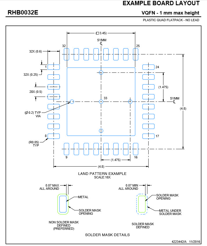
- Sub-optimal sizes for land patterns can be a subtle problem. A land pattern has a slightly different meaning than a footprint, although they are often used However, for PCB assemblers, there’s a huge difference between them that affects manufacturing quality. A footprint is the imprint of a component (that is sometimes loosely termed “real estate”) for the PCB surface area that’s consumed. Think of the footprint as you would if you pressed the component into soft dirt. A land pattern refers to both the outline and the size of the pads required for a component on a PCB. The land pattern will always be larger than the footprint since the land pattern designates the PCB pads where component leads will be landed and soldered. Land patterns are normally identified in component datasheets and should match up accurately with the component footprint. (See Figure 1). Proper land patterns will improve manufacturability.

- Missing notes on height and length requirements on drawings can make it so your board will not fit into the enclosure that may already be fixed. Don’t forget the total height and thickness of your PCB may affect your ability to fit it into a fixed space after components have been stuffed. If your project is size-restricted, then start the design by placing taller components where height clearance is less of a concern. Another tip – note that standard sized PCBs can make a difference in cost versus custom sizes.
- Missing additional information can lead to avoidable issues. The PCB assemblers cannot read your mind. Use a readme.txt file bundled with all the other files to add any special instructions or otherwise missing information. Other files can assist PCB assemblers in interpreting a mistake-free PCB for you, therefore, provide notes, schematics, 3D drawings, and identify any specific features (even how you plan to use the PCB) that will help them form a complete picture.
Meticulously reviewing your project, the PCB layout, and all files and information can make a world of difference in debugging your prototype later. Simple mistakes can burn hours or days in troubleshooting. For instance, choosing the wrong component or putting a component in the incorrect place will complicate the whole process. At best, such mistakes will create delays as the best PCB assembler finds a component marked for a spot that does not match the location’s land pattern. The worst case will be a finished PCB that doesn’t work.
Bundle all your files together by creating a .ZIP or .RAR file. Sending files as multiple separate attachments in different emails can cause delays. Remember that the PCB maker will likely have dozens, hundreds, or even thousands of customers that have submitted their files in the same day or week, with multiple employees handling the incoming requests. A request that’s fractured across two or more emails or uploads may not reach the same person handling your first submission. Bay Area Circuits has a free InstantDFM™ tool that can identify potential production issues in your files before you actually submit them, whether or not you actually use their services.
PCB assembly is placed on hold if it’s missing information, files, special or rare parts for population, or if it includes incomplete information or corrupted files. It’s a universal rule of thumb that any project (across all engineering disciplines) will cost more the longer it takes. Delays almost always add to the total cost, and prior planning prevents poor performance.
[i] https://www.aapcb.com/blog/3-things-affect-your-pcb-assembly-quote/
[ii] https://aapcb.com/knowledge-center/5-common-design-mistakes/


That makes sense that incorrect markings on the PCB would cause some issues. I feel like that could ruin the whole thing is certain components weren’t in place so that would be important to avoid. I’ll have to make sure that I have someone look over the design beforehand if I ever have a PCB made for a project.