Several RISC-V development efforts are targeting applications such as artificial intelligence (AI), machine learning (ML), deep learning (DL), and other high-performance embedded applications. The previous two FAQs in this series considered the capabilities of RISC-V and the near-term risks associated with the technology, and the growing availability of tools that are helping to reduce the risk of using RISC-V. This FAQ looks at some of the options for integrating RISC-V into high-performance systems.
Designers have access to RISC-V technology in several ways. There are companies that offer RISC-V as IP cores that can be used to produce custom cores optimized for specific applications. Other suppliers offer complete RISC-V processors that can be integrated into systems. And in other cases, RISC-V cores have been integrated into SoCs such as FPGAs along with other types of processors and peripherals. The following provides an overview of the types of devices available; it is not comprehensive.
RISC-V ISAs as IP cores
For example, SemiDynamics offers the Avispado core. With its small area and power, Avispado is designed for energy-conscious SoCs targeting ML applications. Avispado supports large memory capacities with its 64-bit native data path. With its complete MMU support, Avispado is also Linux-ready, including multiprocessing. Avispado supports cache-coherent multiprocessing environments. It can support hundreds of cores in a single SoC. Its native CHI interface can be tailored down to ACE or AXI, depending on the application needs.
Avispado supports the upcoming RISC-V Vector Specification 1.0 as well as Semidynamics Open Vector Interface, providing freedom of choice between custom vector units and using Semidynamics offerings. Vector instructions densely encode numerous computations, thereby reducing energy per operation. Vector Gather instructions support sparse tensor weights efficiently, helping ML workloads.
The SiFive Core IP portfolio spans from high-performance multi-core heterogeneous application processors to area-optimized, low-power embedded microcontrollers. SiFive Core IP standard core microarchitectures are based on the RISC-V ISA to provide 64-bit and 32-bit options.
SiFive Core IP can be tuned to specific workloads using SiFive Core Designer, leveraging the flexible generator style SiFive uses to design processor architectures for different performance and efficiency classes. SiFive standard cores based on flexible microarchitecture designs are pre-configured for common use cases and offer a starting point for designing a custom core in SiFive Core Designer.
Cobham Gaisler recently announced a new line of processor IP cores that implement the RISC-V instruction set architecture. The NOEL-V processor IP core, the first product in the family, will be made available on 25 December 2020 for download into Xilinx’ Kintex UltraSCALE FPGAs.
The initial RISC-V product from Cobham Gaisler will be an RV64GC compliant processor IP core, a 64-bit architecture, written in VHDL. The processor will be fully integrated with Cobham’s GRLIB VHDL IP core library. GRLIB offers several interfaces and functions such as high-speed serial interconnect, encryption, compression, and so on, which can be embedded with the RISC-V processor. It will be complemented with the upgrade of the GRMON3 Software Debug Monitor to support the new ISA.
RISC-V as hardware in SoCs, FPGAs, ASSPs, and more
Celerity is an accelerator-centric system-on-chip (SoC) that uses a tiered accelerator fabric to improve energy efficiency in the context of high-performance embedded systems. The SoC is a 5 × 5 mm 385 M-transistor chip in TSMC 16 nm designed and implemented by a team of over 20 students and faculty from the University of Michigan, Cornell University, and the Bespoke Silicon Group (now at U. Washington) as part of the DARPA Circuit Realization At Faster Timescales (CRAFT) program. Celerity currently claims the world record for RISC-V performance; 500B RISC-V instructions per second, beating prior records by 100X.
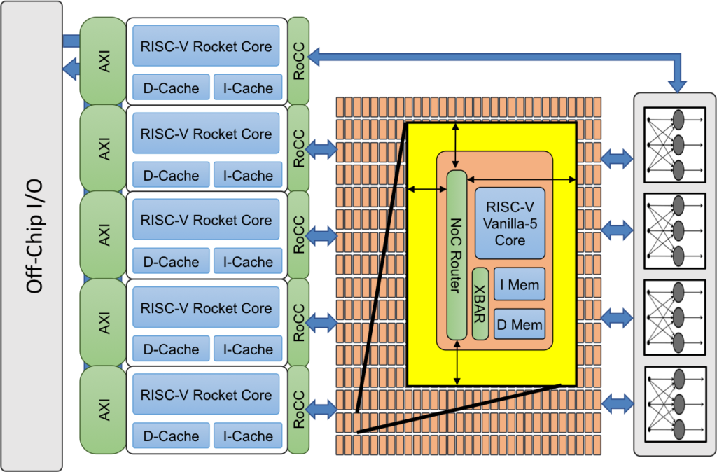
Celerity is a many-core multi-tier AI accelerator. At a high level, the chip comprises three main tiers – general-purpose, massively parallel, and specialization. A tiered SoC enables both high flexibility and higher power efficiency over a typical CPU design. The general-purpose tier is designed for versatility and can perform several tasks – general compute, memory management, and control of the rest of the chip. For this reason, Celerity integrates five high-performance out-of-order RISC-V Rocket cores from the Free Chip Project. The next tier over is the massively-parallel tier, which integrates 496 low-power custom-designed RISC-V cores in a mesh. Those custom cores, called Vanilla-5, are in-order scalar cores that take up 40x less space than a Rocket core. The last tier is the specialization tier that integrates a binarized neural network (BNN) accelerator. All three tiers are tightly linked and interface with DDR memory operating at 400 MHz.
The DARPA CRAFT program, under which Celerity was developed, seeks to shorten the design cycle for custom integrated circuits to months rather than years; devise design frameworks that can be readily recast when next-generation fabrication plants come online; and create a repository of innovations so that methods, documentation, and intellectual property can be repurposed, rather than reinvented, with each design and fabrication cycle. This less expensive design paradigm also could help diversify the innovation ecosystem by making it practical for small design teams to take on complex custom circuit development challenges that are out of their reach today.
Esperanto Technologies is creating a new generation of AI/ML/DL processing solutions claiming unmatched energy efficiency (performance/watt), scalability, and flexibility. The historical limitations on many-core designs have always been complexity and power consumption, but it is now possible to create designs with over a thousand processor cores on one piece of silicon. Esperanto’s high-performance ET-Maxion core is designed to deliver the best single-thread RISC-V performance. The company’s ET-Minion™ core compute array is designed for energy efficiency, delivering TeraFlops and TeraOps of computing.
The rising adoption of the free and open RISC-V ISA drives the need for an affordable, standardized development platform that embeds RISC-V technology and leverages the diverse RISC-V ecosystem. To meet this need, Microchip Technology Inc. is offering the industry’s first RISC-V-based System-on-Chip (SoC) Field-Programmable Gate Array (FPGA) development kit for PolarFire SoC FPGA. Microchip’s Icicle Development Kit for PolarFire (SoC) FPGAs brings together the company’s numerous Mi-V partners to accelerate customer design deployment and commercial adoption across various industries.
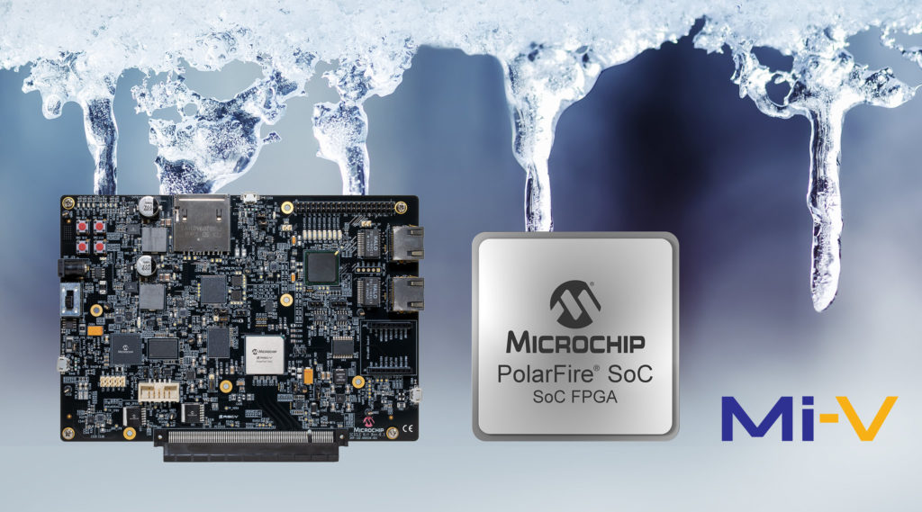
Designers who want to deploy a programmable RISC-V-based SoC FPGA can now start development and evaluate the broad network of RISC-V ecosystem products such as Real-Time Operating Systems (RTOS), debuggers, compilers, System On Modules (SoMs), and security solutions. The Mi-V RISC-V Partner Ecosystem is a continuously expanding, comprehensive suite of tools and design resources developed by Microchip and numerous third parties to support RISC-V designs fully. Microchip’s Icicle Kit for PolarFire SoC and Mi-V ecosystem enables PolarFire SoC FPGAs with:
- RISC-V processor complex from SiFive and embedded trace macro from UltraSoC
- Development tools from Adacore, Green Hills Software, Mentor Graphics, and Wind River
- Commercial RTOS solutions such as Nucleus and VxWorks that complement Microchip’s Linux and bare-metal solutions
- Middleware solutions from DornerWorks, Hex Five, Veridify Security and wolfSSL
- SOM and design services from organizations such as Antmicro, ARIES Embedded, Digital Core Technologies, Emdalo Technologies, Sundance DSP, and Trenz Electronic
Renesas Electronics has entered into a technology IP cooperation with Andes Technology, an advanced supplier of RISC-V based embedded CPU cores and associated SoC development environment. Renesas selected the AndesCore IP 32-bit RISC-V CPU cores to embed into its new application-specific standard products (ASSPs) that will begin customer sampling in the second half of 2021.
The delivery of Renesas’ pre-programmed ASSP devices based on the RISC-V core architecture, combined with specialized user interface tools to set the application programmable parameters, will provide customers with complete and optimized solutions. This capability will eliminate the initial RISC-V development and software investment barrier.
RISC-V and the European Processor Initiative
Looking to future implementation of RISC-V, the European Processor Initiative (EPI) has been funded under the first stage of the Framework Partnership Agreement signed by the Consortium with the European Commission (FPA: 800928), whose aim is to design and implement a roadmap for a new family of low-power European processors for extreme-scale computing, high-performance big-data and a range of emerging applications.
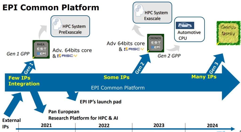
The Accelerator stream for the EPI will develop and demonstrate fully European processor IPs based on the RISC-V ISA, providing power efficient and high throughput accelerator tiles. Using RISC-V allows leveraging open-source resources at both the hardware architecture level and software level and ensuring independence from non-European patented computing technologies. The vector processor architecture will be based on these guiding principles:
- Holistic throughput-oriented vision based on long vectors and task-based models
- Hierarchical concurrency and locality exploitation
- Communication between programming levels
- Look and feel very close to classical sequential programming to ensure productivity
The dedicated unit architecture, on the other hand, will be geared towards a few specific applications. This specificity will be leveraged to explicitly manage the data placement and transfer from and into local scratchpad memories, targeting high-energy efficiency.
The basic building block is a tile containing up to 8 vector processors and specialized units. The processors are coherent, sharing L2 cache banks through a Network-on-Chip, each bank with its associated Home Node agent through a Network-on-Chip. The processors will support RISC-V vector instructions and control the specialized units dedicated to stencil and DL acceleration. The vector and stencil capabilities will address HPC workloads, while the DL units will target AI applications. The tile will be integrated both as a node in the processor mesh and as a stand-alone test chip for demonstration and software debugging purposes.
As shown, designers have multiple paths to using RISC-V ISA technology in high-performance applications such as AI, ML, and DL. The next and final FAQ in this series will expand on the theme of AI and consider “RISC-V for ultra-low-power processing and AI on the edge.”
References:
A Look At Celerity’s Second-Gen 496-Core RISC-V Mesh NoC, WikiChip Fuse
DARPA Circuit Realization At Faster Timescales, DARPA
European Processor Initiative, EPI



Leave a Reply