
Flash memory stores information in an array of memory cells made from floating-gate transistors. Each memory cell resembles a standard metal-oxide-semiconductor field-effect transistor (MOSFET) except that the transistor has two gates instead of one. The floating gate (FG) and the control gate (CG) control the current flowing between the source and drain. The CG resembles the gate in ordinary MOS transistors.
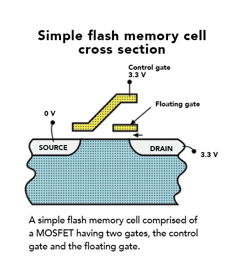 The FG is completely insulated by an oxide layer and sits between the CG and the MOSFET channel. The electrical isolation of the FG traps any electrons placed on it. A charge placed on the FG screens the electric field from the CG, boosting the threshold voltage (VT1) of the cell. This means the CG must see a higher voltage to make the channel conductive. (This higher voltage, often written VT2 in texts, almost always comes from an internal charge pump. Flash chips today need only a single supply voltage.)
Applying a voltage between the threshold voltages (VT1 and VT2) to the CG is all that’s needed to read a value from the transistor. When the channel conducts at this intermediate voltage, it means the FG is uncharged (a charged FG would prevent conduction because the intermediate voltage is less than VT2). This means the gate stores a logical “1.” When the channel doesn’t conduct at the intermediate voltage, the FG is charged, so the gate stores a logical “0.”
Thus current flowing or not flowing through the transistor when the intermediate voltage is asserted on the CG indicates the presence of a logical “0” or “1.” Flash memories with multi-level cells, which store multiple bits per cell, sense the amount of current flow rather than simply its presence or absence to figure out the level of charge on the FG.
Today, there are two main types of flash, NOR and NAND. In NOR flash, each cell has one end connected directly to ground. The other end connects directly to a bit line. The NOR flash moniker comes because the arrangement acts like a NOR gate: when one of the word lines (connected to the cell CG) is brought high, the corresponding storage transistor pulls the output bit line low.
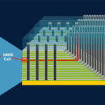
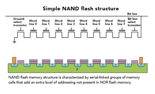 NAND flash also uses floating-gate transistors, but they connect in a way that resembles a NAND gate: several transistors connect in series, and the bit line goes low only if all the word lines are pulled high (above the transistor VT). These groups then connect via additional transistors to a NOR-style bit line array in the same way that single transistors are linked in NOR flash.
A NOR flash might address memory by page and then by word. NAND flash might address it by page, word and bit. Bit-level addressing suits bit-serial applications (such as hard disk emulation), which access only one bit at a time. Execute-in-place applications, on the other hand, require every bit in a word to be accessed simultaneously. This requires word-level addressing. In any case, both bit and word addressing modes are possible with either NOR or NAND flash.
Though it contains additional transistors, NAND flash has fewer ground wires and bit lines that allows a denser layout and greater storage capacity per chip than is available with NOR flash. In addition, NAND flash can typically contain a certain number of faults and still work (NOR flash is generally expected to be fault-free). Because of the series connection and removal of word-line contacts, a large grid of NAND flash memory cells will occupy perhaps only 60% of the area of equivalent NOR cells.

Leave a Reply