FPGAs are complex devices and are being used in more and more systems. The complexity of FPGAs is both a strength and a weakness. It’s a strength because of the many system performance benefits and capabilities they bring for designers to leverage. It’s a weakness because of the complexities of successfully integrating high pin-count FPGAs into high-speed systems. Many things could go wrong – including pin assignments that don’t work in the board layout, signal integrity problems on the board, power and grounding issues, parasitic package inductances, and more. This FAQ will provide a brief overview of some of the challenges and system integration issues that need to be confronted when working with FPGAs, including printed circuit board (PCB) design, software debugging, and power management.
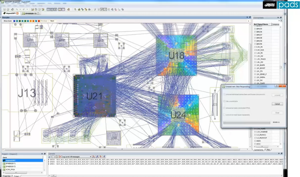
It’s not unusual for an FPGA to go through four or more design iterations before arriving at a “final” I/O pinout. One of the challenging aspects for FPGA users can be waiting for the actual “final” pinout; many performance factors can arise during system integration that may require a re-spin of the FPGA layout. And considering that about one-third of designs include multiple FPGAs, the challenges can multiply. PCBs used in FPGA-based systems are complex and sophisticated interconnect systems. Co-design, communication, and cooperation between FPGA developers and PCB designers can prevent many potentially catastrophic changes to the PCB physical design as the FPGA goes through multiple iterations.
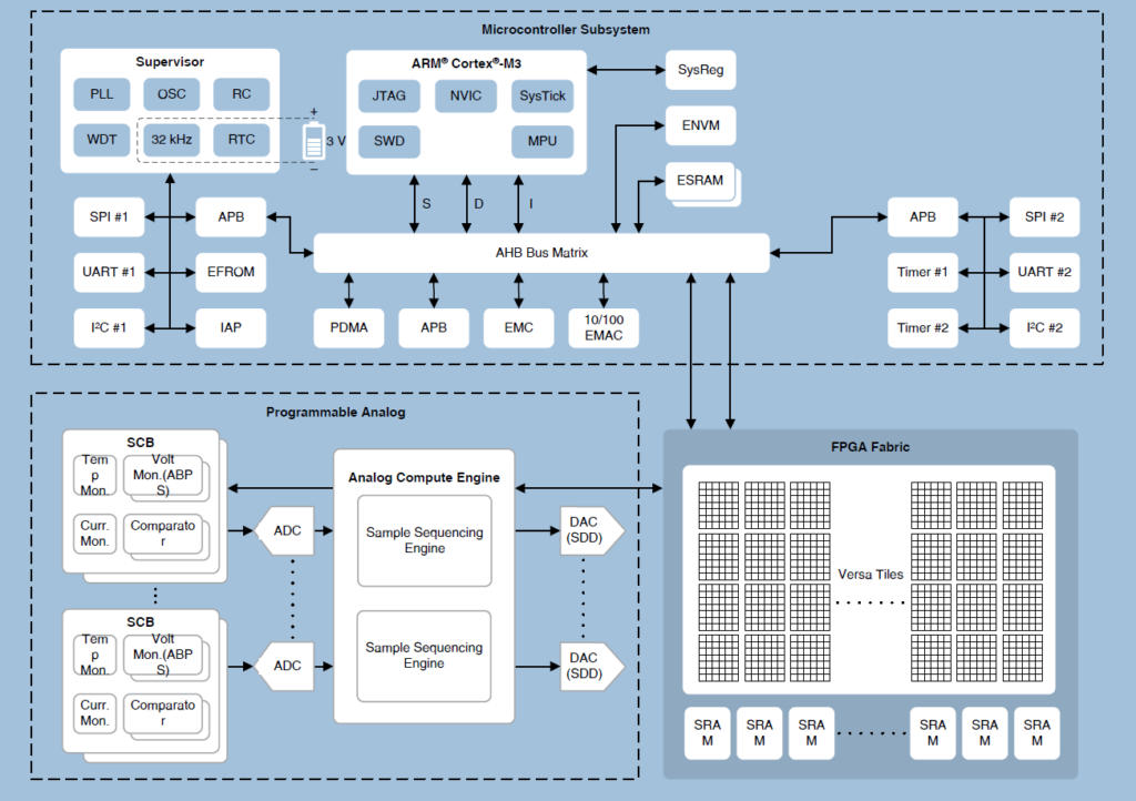
The greater flexibility of FPGAs compared with ASIC- or CPU-based designs can be important. Various architectural approaches can be created and tested until an optimal design is achieved. FPGAs with on-chip processors make it possible to tradeoff discrete CPU-based processing with embedded FPGA-based acceleration functions. Properly implemented, the time required for design, testing, and validation of new designs can be reduced.
FPGA support for hardware and software cores for standard functions such as various communication buses can simplify the testing needed for those standard functions. FPGAs can also include on-chip ARM processors. Existing processor code can be ported to the design, and new code created in parallel with the system design.
A large selection of code libraries, drivers, functional APIs, RTOS, and more are available to FPGA users when integrating standard processors and standard interface buses. That can speed the development process and enable the use of standard simulation and testing solutions, further speeding development times. Finally, FPGAs themselves can help manage debugging due to additional hardware features included specifically for that activity.
Debugging issues with FPGA designs
As a result of FPGAs’ complex and extensive functional capabilities, debugging a new design can encompass 50% or more of the overall design time. Timing issues at the system level can be a serious challenge. FPGAs typically have multiple timing domains, and a common source of problems is asynchronous errors, especially across timing domains. These can be especially challenging and often appear only when a specific set of circumstances such as specific data patterns exist.
Interference between multiple power rails and low signal fidelity between adjacent ICs can also be causes of timing issues. Cross-talk, reflections, general signal noise, and EMI can all contribute to timing violations. Correctly fabricated PCBs can be subject to various disruptions from power-related issues such as voltage transients, load surges, and excess power dissipation.
Like high-performance systems in general, the increasing complexity of FPGA-based systems drives the need for additional passive devices such as resistor terminations and decoupling capacitors to help address noise and signal issues. Embedded passives can be found on the inner layers of more and more PCBs since they reduce interconnect dimensions, board area and provide superior performance.
Banks of I/Os on FPGAs are dedicated to multi-gigabit communications. Achieving clean data transmissions at those speeds requires the precision implementation of PCB interconnects and careful matching and controlling driver and receiver operating characteristics. At multi-GHz frequencies, even small vias can look and behave like antennas, degrading signal quality. For example, the PCI Express bus specification strongly recommends using ewer than two vias per trace and trace length matching to within a tolerance of 0.025%.
Co-design, communication, and cooperation between FPGA developers and PCB designers can also address complexities in FPGA powering. FPGAs’ flexibility allows designers to assign different voltages, drive strengths, and slew rates to different pins. Without following FPGA vendor specifications and guidelines, there can be ringing and crosstalk introduced on the PCB. In addition, power supplies can introduce random switching noise that contributes to jitter or variations in the timing of bit transitions with respect to the data-rate clock.
Power supply concerns and challenges
The power supply requirements in FPGA datasheets are growing in complexity as well as in importance. A large FPGA can have over 12 power rails, with some rails requiring 40-50A of current. Among the considerations for FPGA power system design are:
- Current needs of individual power rails
- Sequencing the various voltage rails
- Monotonic rise of the various voltages
- High voltage accuracies
- Fast transient responses
Common FPGA powering solutions include using a distributed power architecture where a relatively high intermediate bus voltage such as 48Vdc or 12Vdc is delivered to the area of the FPGA, followed by various non-isolated point-of-load (PoL) dc/dc converters. This can be particularly useful for delivering the high-current rails. In addition, power management ICs (PMICs) that contain multiple dc/dc converters on a single chip can be used. In practice, there is often a mix of discrete PoLs and one or more PMICs.
FPGAs require a range of voltage rails from sub-1V up to 3.3V, sometimes higher. Examples of voltage needs include: If a particular bank has a DDR2 SDRAM connected, it will require a 1.8V drive and a 0.9V reference; a 2.5V power bus is needed instead of 1.8V if an LVDS bus is connected to the bank; And, while DIMMs usually require a 1.8V SSTL signal, various types of I2C signals could require a different voltage.

FPGAs often require that the various voltage rails power up and down in specific sequences. To prevent damage, it is usually specified that the core voltages come up before the I/O voltages, and some auxiliary functions may need to be powered up after the I/O voltages. In addition to sequencing, the various voltage rails are required to rise monotonically during startup. That requires that the voltages only rise during start-up; they cannot rise for a period, fall, then rise again.
An additional power controller IC may be needed. PMBus is often used to control the various dc/dc converters. These power management ICs can also integrate extensive digital monitoring and power system management, including protection circuits for overtemperature and overcurrent, short circuits, and UVLO faults.
At the end of the startup period, the various voltages are subject to strict regulation and accuracy demands. FPGAs can power up and down rapidly and draw high currents upon startup. As a result, they demand extensive voltage decoupling on the high-current inputs. Ceramic capacitors up to 1mF can often be found on the input pins. Designers should carefully review the maximum output capacitances specified for the various switching regulators and LDOs used in an FPGA design. Too much capacitance can degrade the performance of power converters.
The selection of the correct capacitors for the input pins can also impact the voltage accuracy. Voltage accuracies of 3% are commonly seen in FPGA power specifications. Various types of ceramic capacitors can have widely varying values under changing operating conditions. It is important to use capacitors that are sufficiently stable over the anticipated operating conditions.
There are many challenges to deal with when integrating FPGAs into systems – including pin assignments that don’t work in the board layout, signal integrity problems on the board, power and grounding issues, parasitic package inductances, and more. This FAQ has provided a brief overview of some of the challenges and system integration issues that need to be confronted when working with FPGAs, including PCB design, software debugging, and power management.
References:
Board-level considerations, Microsemi
In-Circuit FPGA Debug – Challenges and Solutions, Microsemi
Power management for FPGAs, Analog Devices
Printed Circuit Board (PCB) Design Checklist, Xilinx
Successfully Designing FPGA-Based Systems, Cadence



Leave a Reply