
A System on Chip or an SoC is an integrated circuit that incorporates a majority of components present on a computer. As the name suggests, it is an entire system fabricated on a silicon chip. The beauty of an SoC is that it integrates all the components on a single substrate. In semiconductors, a substrate is a thin film of silicon used to fabricate integrated circuits. In contrast to the traditional motherboard, SoC integrates the replaceable components onto a single chip, thereby reducing the size and increasing efficiency.
Along with the integrated circuit, an SoC includes software and an interconnection structure for integration. The hardware-software integration approach makes the SoC smaller in size, allows for less power consumption, and more reliable than a standard multi-chip system.
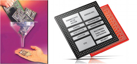
Components of an SoC
SoCs can be identified as the following types: built around a microcontroller, build around a microprocessor, built for specific applications, and programmable SoCs (PSoC). The integral parts of an SoC include a processor, primary and secondary memory storage and input/output ports. The other vital components include a graphics processor unit (GPU), a WiFi module, Digital Signal Processor (DSP), and various peripherals such as USB, Ethernet, SPI (Serial Peripheral Interface), ADC, DAC, and even FPGAs. Usually, it has multiple cores. Depending on various deciding factors and preferences, the core can be a microcontroller, microprocessor, DSP, or even an ASIP (Application Specific Instruction- set Processor). ASIPs have instruction sets based on a particular application. Usually, SoCs use ARM architecture, which is a family of RISC (Reduced Instruction Set Computing), which requires less digital design, thereby making it compatible for embedded system use. The ARM architecture is much more power-efficient than processors like the 8051 because, in contrast to processors using the CISC architecture, processors with RISC architecture require fewer transistors. This also reduces heat dissipation and the cost.
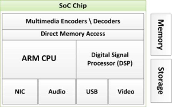
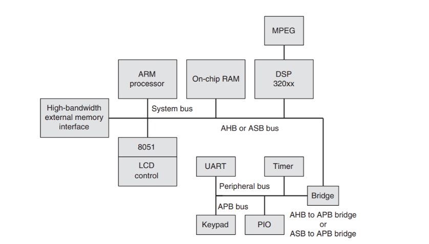
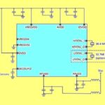
The following diagram shows an example of an SoC block diagram.
Processor
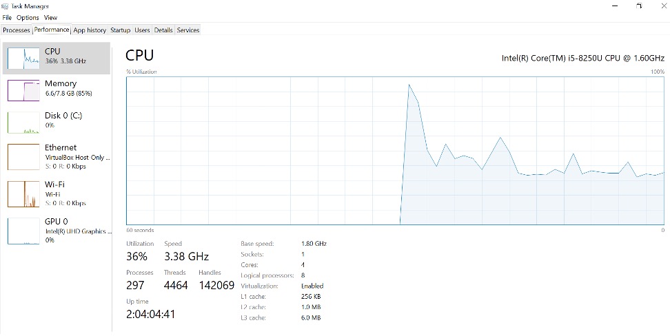
At the heart of the SoC is its Processor. It usually has multiple processor cores. Multiple cores allow for different processes to run at the same time, which increases the speed of the system as it enables your computer to perform multiple operations at the same time. Basically, the operating system sees the multiple cores as multiple CPUs, which increases performance. As multiple cores are fitted onto the same chip, there is less latency, which is because of faster communication between the cores. A multiple core system has only one CPU socket with multiple cores. For example, the following system has four cores and one socket.
Because of hyper-threading, to an operating system, a single-core appears as two logical units. Hyper-threading allows sharing of physical resources between two CPUs.
Digital Signal Processor (DSP)
Digital Signal Processor (DSP) is a chip optimized for operations for digital signal processing. This includes operations for sensors, actuators, data processing, and data analysis. It can be used for image decoding. The use of DSP saves CPU cycles for other processing tasks, which increases performance. Dedicated DSPs are more power-efficient, which makes them befitting for use in SoCs. The instruction set used for DSP cores is SIMD (Single Instruction, Multiple Data) and VLIW (Very Long Instruction Word). The use of this architecture allows for parallel processing of instructions and superscalar execution. DSPs are used to perform operations like Fast Fourier Transform, convolution, multiply-accumulate.
Memories on an SoC
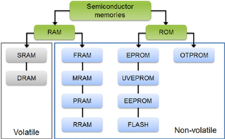
SoCs have memories based on the application. The memories are semiconductor memory blocks for computation purposes. Semiconductor memory usually refers to Metal Oxide Semiconductor memory cells, which are fabricated on a single silicon chip. The types of memories are:
- Volatile memories: Memories that lose data after power off. In other words, they need a constant power source to retain information. Volatile memories are faster and cheaper, which is why they are chosen frequently.
RAM is a type of volatile memory. The most common RAM used are SRAM (Static RAM) and DRAM (Dynamic RAM). SRAM is made of memory cells which consist of either 1,3 or 6 transistors (MOSFETs). In contrast, DRAM has only one MOSFET and a capacitor which is charged and discharged according to the state of the FET. However, DRAM is prone to capacitor leakage currents. One significant advantage of DRAM is that its cheaper than SRAM. If an SoC has a cache hierarchy, SRAM is used for cache and DRAM is used for the main memory. This is because cache requires a faster type of memory as compared to the main memory.
There are RAM types designed for non-volatile function as well. These are FRAM (Ferroelectric RAM), MRAM (Magnetoresistive random-access memory), which stores data in magnetic states, PRAM (Parameter Random Access Memory), which is used in Macintosh computers to store system settings including the display and time-zone settings. Other than these, there is RRAM (Resistive Random Access Memory), which has a component called memristor. A memristor is a resistor whose voltage varies as per the applied voltage.
- Non-volatile memories: Memories that retain information even in the absence of a power source. ROM (Read Only Memory) is a kind of non-volatile memory. Types of ROM include EPROM (Erasable Programmable Read-Only Memory), which is an array of floating-gate transistors. UVROM(Ultra-Violet Erasable Programmable Read-Only Memory), which is erased using UV light and reprogrammed with data, EEPROM(Electrically Erasable Programmable ROM) and flash.
The type of memory selected depends upon the design specifications and application.
Companies that primarily manufacture semiconductor memories are Micron Technology, Intel Corporation, Western Digital.
On-chip communication
Traditionally, bus architecture was used to communicate between the SoC’s execution units. However, these days, Network-On-Chip interconnect technology has emerged as a trend to overtake the bus architecture.
A popular example of bus communication is the AMBA (Advanced Microcontroller Bus Architecture) bus protocol by ARM. The bus architecture is used to drive data between components. On-chip bus architecture can be classified as a shared bus, hierarchical bus, and ring topologies. Different companies have designed different architectures as per the chip design and application. A few examples are Altera AVALON, IBM CORECONNECT, WISHBONE by Silicore Corporation.
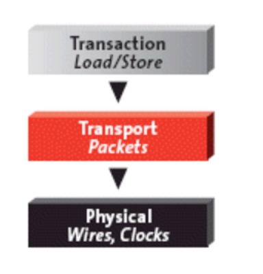
The Network-On-Chip employs system-level network techniques for on-chip traffic management. The NOC is a homogeneous, scalable switch fabric network that is used to transport multi-purpose data packets. This architecture is layered in nature with user-defined technology. The communication takes place over a three-layer communication scheme, namely Transaction, Transport, and Physical.
The aim of a NOC interconnect fabric is to reduce the wire routing congestion on-chip, better timing closure, a standardized way to make changes various IPs to the SOC design. NOC architectures have proven to be more power-efficient and can match throughput requirements.
External interfaces
SOC interfaces defer as per the intended application. The external interfaces are commonly based on communication protocols such as WiFi, USB, Ethernet, I2C, SPI, HDMI. If required, analog interfaces may be added for interfacing with sensors and actuators.
Other components
Other components necessary for a fully functioning SOC are timing sources like clocks, timers, oscillators, phase lock loop systems, voltage regulators, and power management units.
SoC design flow
The SoC design flow is aimed at architectural co-design, which designs both hardware and software at the same time. The design flow must take into account optimization goals and various constraints. The diagram below is an example of an SoC design flow from specifications to fabrication. Separate teams perform each of the steps involved in manufacturing an SoC.
An SoC is fabricated using MOS technology. Today, the smallest MOS technology is the 3nm technology developed by TSMC and Samsung. However, most devices today use 10nm technology. The fabrication process involves the netlist generation of design, followed by the physical design flow. Throughout the process, special attention is paid to the static timing analysis (STA), which is the computation of timings in a digital circuit. STA is also used to validate timing performance and check for any timing violations. Timing violations can lead to metastability, which is when the flip-flops in a digital circuit are in an unknown state (neither 1 nor 0).
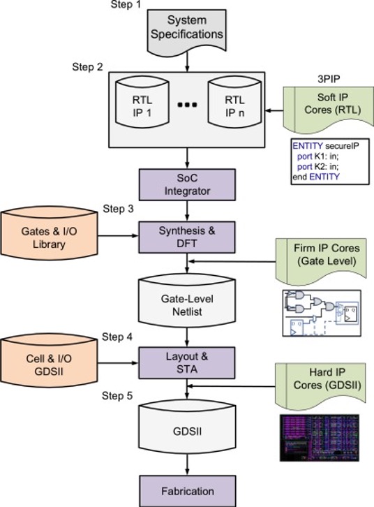
In Step 1 of fabrication, the design specifications are analyzed, and a list of IPs required to perform the specifications is generated. These IPs or Intellectual Properties are usually outsourced to third-party IP vendors. These IPs can be Soft Cores, Hard Cores, or firm cores, depending on the level of flexibility for changing parameters. IPs can be made by the same company as well.
In Step 2, the IPs are integrated to generate an RTL description of the entire design. RTL stands for Register Transfer Level, which includes the use of various Hardware Descriptive Languages like Verilog, System Verilog, and VHDL. RTL models synchronous digital circuit between hardware registers.
In Step 3, a gate-level netlist is generated by the SoC integrator. A gate-level netlist contains data about the logical connectivity of standard cells, including for combinational, sequential cells, and nets. A net is a group of two or more interconnected components. Design-For-Test (DFT) tools are used to improve testability.
In Step 4, the gate-level netlist is converted into a layout based on the physical design process.IP cores can also be imported at this stage. Physical design involves converting circuit representations of a design into geometric shapes, which leads to functioning components after manufacturing.
In Step 5, assuming that Static Timing Analysis and power analysis are complete, a final layout is developed and send for fabrication.
In Step 6, the fabricated chip is checked in assembly. Chips are thoroughly checked for logical correctness before this step. This checking is called functional verification and accounts for a significant portion of the process. To perform verification, languages like SystemC, System Verilog are increasingly becoming popular to accommodate the complexity.
It is important to remember that making any changes to a chip after fabrication is very difficult and costly. Hence, emulation (prototyping) of design is performed before fabrication. This is popularly done using FPGAs (Field Programmable Gate Array) because it is reprogrammable and allows debugging.
Advantages & disadvantages of SoC
The main aim of an SoC is to minimize external components. Hence, it has the following advantages over a Single Board Computer:
- Size: The SoC is the size of a coin. Due to the rapidly decreasing size of MOS technology, SOCs can be made very small while being able to perform complex tasks. The size does not impact the features of the chip.
- Decreased power consumption: An SoC is optimized for low-power devices like cell-phones. Low power consumption results in higher battery capacity in cell-phones.
- Flexibility: SoCs are easily reprogrammable, which makes them flexible. They so allow the reuse of IPs.
- Reliability: SoCs offer high circuit security and reduced design complexity.
- Cost Efficient: Mainly due to fewer physical components and design reuse
- Faster circuit operation
SoCs pose some disadvantages as well:
- Time Consuming: The entire process from design to fabrication can take between 6 months to 1 year. Hence, the time to market demand is very high.
- Design Verification requirements are very high and consume 70% of the total time. DV is tedious due to the increasing complexity of SoC design.
- Availability and compatibility of IPs play a very significant role, which can add to the time to market.
- Exponentially increasing fabrication costs.
- For low volume products, SoC may not be the best option.
Applications
The most common application of SOCs today is in mobile applications, including smartphones, smartwatches, tablets. Other applications include signal speech processing, PC interfaces, data communication. SoCs are being applied to personal computers as well due to the integration of communication modules like LTE and wireless networks onto the chip.
The most popular SoCs in the market today are manufactured by Qualcomm Technologies for smartphones, smartwatches, and the upcoming 5G network compatibility. Other manufacturers include Intel Technology, Samsung Inc, Apple Inc., among many others.

Leave a Reply