by Jon Wilder
 As some of you have noticed, the internal RAM in the PIC 16F appears to be arranged in “banks”. Each bank holds 128 RAM registers total. The first 128 RAM locations are in bank 0, the next 128 RAM locations are in bank 1, so on and so forth.
But hold on…is this REALLY the case? If it is, then why is it that when we indirect address via the FSR pointer register that we can access 256 RAM locations without having to bank select?
Because this isn’t what’s really going on.
iRAM on a PIC 16F is a contiguous space. It starts at address 0x000 and ends at 0x1FF. However, some locations within this space are unimplemented. The datasheet states that iRAM is divided up into 4 banks of 128 registers each. Why is this?
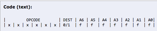
The reason is because there is a limitation in the instructions that the PIC uses to address iRAM locations (basically all of the instructions which have an “f” in them). Byte-oriented instructions which address the registers are in the format of –
Bit-oriented operations (bsf, bcf, btfss and btfsc) are in the format of –
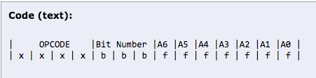
Notice AD0-AD6…that’s only 7 address bits!
Basically, instructions which directly address the iRAM register locations can only provide 7 of the address bits. Since 7 bits can only count to 0x7F (decimal 127), this limits the instruction itself to only access 128 RAM locations on its own…hence the limitation.
So how can we overcome the limitation so that we can address the entire iRAM space? With the addition of two more bits of course, but where would they come from?
Simple…the STATUS register!
We’ve all heard them referred to as the “bank select” bits but this is just a convention that Microchip decided to use for its “register banking” concept. Bits RP1 and RP0 (Register Page 1 and Register Page 0 respectively) serve as the upper 2 address bits for instructions which directly address the iRAM locations.
So say for instance we wanted to move a value in W to register TRISA, which has iRAM address 0x85 (b’010000101). The instruction could not supply the leading “01” in the address, so these two bits must come from register bits RP0 and RP1. So prior to writing the contents of W to register TRISA, we must first execute these two instructions –
bsf STATUS,RP0
bcf STATUS,RP1
This makes bit RP1 a 0 while making bit RP0 a 1, which gives us the leading “01” in TRISA’s address.
Now we want to write to PORTA, which resides at iRAM address 0x05 (b’000000101′). Now the leading two bits must be cleared to access location 0x05 –
bcf STATUS,RP0
bcf STATUS,RP1
This clears both of our RP bits, giving us the two leading zeros at the beginning of our instruction, while the remaining 7 bits come from the instruction itself.
With indirect addressing using the FSR register, we only need 1 more bit. This is because the FSR is an 8 bit register so it can address up to 256 iRAM locations on its own. Its 9th bit comes from bit IRP (Indirect Register Page) in the STATUS register.
With a more conventional processor like the Intel 8051, a mov instruction is 8 bits long, followed by 1 or 2 more bytes that provide the address(es) that the mov instruction is being executed on. With an instruction set of this nature, no iRAM ‘banking’ is required. But since the PIC is a RISC processor with a single 14 bit instruction word, there will be limits to what can be done and how things must be done, and this is one of them.
If we were to use the FSR to indirectly address register TRISA, we could simply load the FSR with the value of 0x85, load W with the immediate value to write to TRISA, then load the value in W into the INDF register without having to bank select. This is because register FSR is an 8 bit register and can supply 8 of the 9 address bits on its own. However, we must ensure that bit IRP in the STATUS register is clear prior to doing this otherwise we would end up writing to iRAM register address 0x185 instead of 0x085.
So there you have it…PIC 16F register banking explained.
“Not sure what Microchip was thinking”, but “PIC12” and “PIC14” are terms used to describe CPU architecture, and “PIC12” and “PIC16” devices might be PIC12 or PIC14 architecture. “Clear as mud!”
The register bank scheme described here is a good explanation for PICs with a PIC14 instruction set and architecture.The PIC16F505 (and some others) Register Bank Scheme is different, the device has a PIC12 architecture but has extended it using code-page selection bits in the STATUS register and Register Bank selection using the upper bits of the FSR register. As the FSR only requires 5-bits to address each bank, the upper 3bits serve as Bank Selection both for Indirect Addressing and for Direct Addressing. So- you need to track the current value of the FSR to know which register is actually being accessed in each instruction.This is an easier task when writing in a high-level language, but can complicate things when debugging in MPLAB. “as I learned!”
not a neat way to access memory