• Skip to primary navigation
  • Skip to main content
  • Skip to primary sidebar
  • Skip to footer

Microcontroller Tips

Microcontroller engineering resources, new microcontroller products and electronics engineering news

  • Products
    • 8-bit
    • 16-bit
    • 32-bit
    • 64-bit
  • Applications
    • 5G
    • Automotive
    • Connectivity
    • Consumer Electronics
    • EV Engineering
    • Industrial
    • IoT
    • Medical
    • Security
    • Telecommunications
    • Wearables
    • Wireless
  • Learn
    • eBooks / Tech Tips
    • EE Training Days
    • FAQs
    • Learning Center
    • Tech Toolboxes
    • Webinars/Digital Events
  • Resources
    • Design Guide Library
    • DesignFast
    • LEAP Awards
    • Podcasts
    • White Papers
  • Videos
    • EE Videos & Interviews
    • Teardown Videos
  • EE Forums
    • EDABoard.com
    • Electro-Tech-Online.com
  • Engineering Training Days
  • Advertise
  • Subscribe

Large-format CMOS image sensor provides 127.68-Mpixel sensing

March 12, 2021 By Redding Traiger Leave a Comment

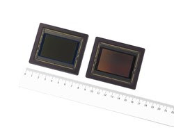
Sony Corporation announced today the upcoming release of a large format 56.73mmdiagonal CMOS image sensor “IMX661” for industrial equipment with a global shutter function and the industry’s highest*1 effective pixel count of 127.68 megapixels.*2

This product features an increased pixel count that yields an optical size nearly 10 times larger than the common 1.1-type image sensor corresponded to the C mount*3 for industrial equipment. It also features Sony’s original global shutter pixel technology “Pregius”, which enables the capture of motion distortion-free images. Furthermore, Sony’s original device configuration and interface technology employed enables high-speed image readout at a data rate nearly four times faster*4 than conventional products.

Sony expects that the new sensor, when used in industrial equipment cameras for a wide variety of applications, will help to solve a variety of complex challenges, thereby contributing to the development of the industry.

Needs for automation, labor-saving, and other benefits of digital transformation continue to grow in recent years in various fields of industrial equipment. This has accelerated the adoption of cameras for a wide variety of applications, driving demand for CMOS image sensors with higher imaging performance.

The new product couples Sony’s Pregius technology with the 3.6-type (56.73mm diagonal) large optical size, delivering an increased pixel count and motion distortion-free imaging. The original device configuration, which employs a chip-on-wafer process, together with Sony’s original interface technology, enables high-speed readout nearly four times faster than conventional products*4 in full-pixel readout mode. This design delivers highly efficient imaging that captures a wide viewing angle with no motion distortion in a single imaging operation. It also improves recognition precision thanks to high-resolution imaging and delivers a high level of processing performance. It can contribute to solutions for a variety of industrial equipment applications, for example, inspection processes for the production of displays and electronic substrates, wide-area monitoring, and aerial photography, where its improved precision and the quicker readout will help meet the need for a high level of productivity.

You may also like:


  • Sentient robots and artificial intelligence

  • LCD contrast vs temperature
  • FPGAs
    What are the application considerations when selecting FPGAs?

  • Tips on designing smart home devices – Part 1

Filed Under: Industrial, Products, Security, Sensor modules, Tools Tagged With: sony

Reader Interactions

Leave a Reply Cancel reply

Your email address will not be published. Required fields are marked *

Primary Sidebar

Featured Contributions

Five challenges for developing next-generation ADAS and autonomous vehicles

Securing IoT devices against quantum computing risks

RISC-V implementation strategies for certification of safety-critical systems

What’s new with Matter: how Matter 1.4 is reshaping interoperability and energy management

Edge AI: Revolutionizing real-time data processing and automation

More Featured Contributions

EE TECH TOOLBOX

“ee
Tech Toolbox: Internet of Things
Explore practical strategies for minimizing attack surfaces, managing memory efficiently, and securing firmware. Download now to ensure your IoT implementations remain secure, efficient, and future-ready.

EE Learning Center

EE Learning Center

EE ENGINEERING TRAINING DAYS

engineering
“bills
“microcontroller
EXPAND YOUR KNOWLEDGE AND STAY CONNECTED
Get the latest info on technologies, tools and strategies for EE professionals.

RSS Current EDABoard.com discussions

  • Antiparallel Schottky Diodes VDI-Load Pull
  • interfacing gsm and gps in proteus
  • 12VAC to 12VDC 5A on 250ft 12AWG
  • What is the purpose of the diode from gate to GND in normal Colpitts oscillator Circuits?
  • My array have wrong radiation pattern

RSS Current Electro-Tech-Online.com Discussions

  • Actin group needed for effective PCB software tutorials
  • Kawai KDP 80 Electronic Piano Dead
  • Doing consultancy work and the Tax situation?
  • How to repair this plug in connector where wires came loose
  • Lightbox circuit

DesignFast

Design Fast Logo
Component Selection Made Simple.

Try it Today
design fast globle

Footer

Microcontroller Tips

EE World Online Network

  • 5G Technology World
  • EE World Online
  • Engineers Garage
  • Analog IC Tips
  • Battery Power Tips
  • Connector Tips
  • DesignFast
  • EDA Board Forums
  • Electro Tech Online Forums
  • EV Engineering
  • Power Electronic Tips
  • Sensor Tips
  • Test and Measurement Tips

Microcontroller Tips

  • Subscribe to our newsletter
  • Advertise with us
  • Contact us
  • About us

Copyright © 2025 · WTWH Media LLC and its licensors. All rights reserved.
The material on this site may not be reproduced, distributed, transmitted, cached or otherwise used, except with the prior written permission of WTWH Media.

Privacy Policy