By Chris Francis
Some of the newer Microchip PIC microcontrollers feature “configurable logic cells” or CLC. What are they and how useful are they?
They appear in a small selection of the PIC devices and are a programmable combination of gates and latches that can be combined to produce an output. Rather than being a general purpose logic block which can be connected to anything and configured to do anything, there is quite a rigid combination of possible connections. That is not to say that there are not many combinations available, but you do have to carefully read the datasheet to see what you can and cannot do.
The CLC varies depending on the microcontroller so the number of CLCs available will differ as do the connection possibilities. For example, this is the PIC24FV16KM204:
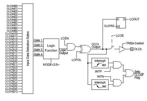
Some of the Microchip documentation is a little out of date it would seem. For example, in DS41631B it says “For all CLC modules, there are eight signals available as inputs to the configurable logic cell, and these eight input signals may vary from device to device. Nevertheless, only four can be selected at any one time.” However, the PIC16F1717 has a choice of 32 inputs within the CLC configuration tool version 3.0.0.4 rather than 8 with the PIC24FV16KM204.
While the PIC24FV16KM204, shown above, looks like it has 32 inputs, the detail of the 32 inputs shows that only one out of each group of 8 CLCIN[x] signals can be selected as one of the four inputs to the CLC logic:
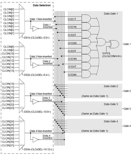
By contrast, any of the 32 can be connected on the PIC16F1717 – even more if PPS (Peripheral Pin Select) is taken into account.
Future “intelligent analog” devices such as the PIC16F1717 look like they will give considerably more options with less restriction on what can be routed to the four logic inputs – we will need to wait for the release of full datasheets to be certain. Some of the clues to future devices are from the CLC configuration software available from Microchip’s web site rather than data sheets. The options with the PIC24FV16KM204 are far more restricted than the PIC16F1717. This can be seen by using the Microchip CLC configuration tool and selecting the required device then looking at the inputs available for each gate from the drop-down box. It can also easily be determined from the data sheet e.g. for Data 4 above (DS4x in CLCxSEL<14:12>) the choices are:
DS4<2:0>: Data Selection MUX 4 Signal Selection bits
111 = MCCP3 Compare Event Flag (CCP3IF)
110 = MCCP1 Compare Event Flag (CCP1IF)
101 = Digital logic low
100 = CTMU Trigger interrupt
For CLC1:
011 = SPI1 SDIx
010 = Comparator 3 output
001 = CLC2 output
000 = CLCINB I/O pin
For CLC2:
011 = SPI2 SDIx
010 = Comparator 3 output
001 = CLC1 output
000 = CLCINB I/O pin
You have two CLC modules in this device and the available inputs to each gate depend on which CLC module you are configuring.
Once you have selected the (up to 4) inputs for the logic functions, you have a choice of what logic functions you use. There are 8 combinations – some only combinatorial:
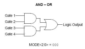
others with a latch:
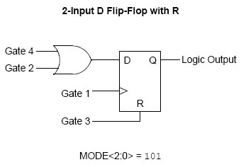
If you select a J-K or transparent latch with SR then you get no logic gates – only the latch.
So, what can you use it for? Almost all of the uses suggested by Microchip make use of the CLC with other modules to give other functions or improved functions such as combining the NCO (numerically controlled oscillator) with the CLC to implement a high resolution PWM. Another example uses the CLC with the NCO to create a Manchester decoder (which feeds the output to the SPI module for deserializing). However it needs three CLC blocks (more than the PIC24FV16KM204 has) and quite a few pins as signals need routing outside the chip as internal routes aren’t available.
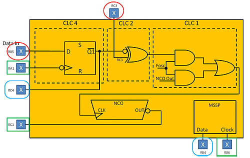
For example, “data in” is on RB5 going to CLC4 and also needs to connect to CLC2. However, RB5 cannot connect to CLC2 so RC3 is used and the pins for RC3 and RB5 externally connected. This seems a bit crude and reminds me of some of the problems of routing early FPGAs, although I have come across similar problems with the analog routing of Cypress PSoC devices.
A VCO (voltage controlled oscillator) with linear frequency output again uses the NCO in conjunction with the CLC module. A delay block/debouncer example using the CLC in the PIC10F322 is rather simplistic and the CLC is used simply as an inverter or “pass-through” with no delay when the delay is not required.
In summary, the CLC is a bit of “glue” logic. It is fairly limited as to what it can be used for on its own. It is not as flexible as an old fashioned PAL (programmable array logic) device, partly because of the limited connections available, but also because of the limited amount of logic available. Its use is more likely to be as “glue” for the built in blocks such as the NCO and PWM as shown in the Microchip examples. Something like the Cypress PSoC has a more powerful range of digital blocks and functions and also more flexible logic routing, although still not providing true PAL functionality. The PSoC is a different type of processor though, even ignoring the analog functionality. The PSoC relies on the configurable digital logic for many of the functions that are built in to other processors such as PWM, SPI and UART. The real improvements in the functionality of the PIC microcontrollers with CLC are really in the improved peripherals such as the NCO and CWG (complementary waveform generator), with the CLC providing a little extra logical glue to assist in their use rather than providing a useful function in their own right – they are too limited for that.
Leave a Reply