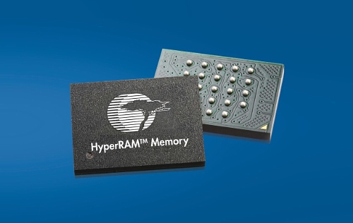
Cypress Semiconductor Corp. today announced sampling of a new high-speed, self-refresh Dynamic RAM (DRAM) based on Cypress’s low-pin-count HyperBus™ interface. The 64Mb HyperRAM™ serves as an expanded scratchpad memory for rendering of high-resolution graphics or calculations of data-intensive firmware algorithms in a wide array of automotive, industrial and consumer applications. The devices operate with a read/write bandwidth of up to 333 MBps and are available in 3V and 1.8V supply voltage ranges.
When paired with a Cypress HyperFlash™ NOR Flash memory, HyperRAM enables a simple and cost-effective solution for embedded systems where both the flash and RAM reside on the same 12-pin HyperBus. Traditional systems with an SDRAM and Dual-Quad SPI solution require upwards of 41 pins on two buses for data transactions. The HyperRAM and HyperFlash solution reduces pin count by at least 28 pins, decreasing design complexity and lowering PCB cost. HyperRAM is an ideal solution for automotive clusters and infotainment, communication equipment, industrial applications and high-performance consumer products. More information on the 64Mb HyperRAM is available athttp://www.cypress.com/
“With the rapidly growing usage of high-resolution graphics and data-intensive applications in a wide range of systems, we see a growing need in the market for a simple, high-performance DRAM that provides external scratchpad memory for controllers with limited onboard RAM,” said Rainer Hoehler, Vice President of the Flash Business Unit at Cypress. “Our new 64Mb HyperRAM addresses this requirement with the low-pin-count HyperBus interface and its industry-leading read/write bandwidth. In addition to lower PCB cost, HyperRAM lowers MCU costs by reducing the number of pins needed compared with other DRAM solutions.”
To accelerate product design cycles, Cypress offers customers and partners a HyperBus Master Interface Controller IP Package. This controller IP helps designers add support for HyperBus to their Field-Programmable Gate Array (FPGA), Application-Specific Integrated Circuit (ASIC) or Application-Specific Standard Product (ASSP) host controller platform. The Controller IP supports both HyperRAM, as well as HyperFlash products, and is free of charge and royalty-free.
Availability
The Cypress 64Mb HyperRAM is sampling now with production beginning in the third quarter of 2016. The devices will be available in a 24-ball, 6-mm by 8-mm ball grid array (BGA) package.
About Cypress HyperFlash Memory
High-density (128Mb to 512Mb) HyperFlash NOR Flash memories deliver the bandwidth required for the highest-performance embedded systems found in automotive instrument clusters, automotive infotainment systems, communication systems and industrial applications. They deliver the highest read bandwidth at 333 MBps, more than four times faster than Quad SPI NOR flash, with one-third the number of pins of parallel NOR flash. More information on HyperFlash is available at www.cypress.com/hyperflash.
About Cypress HyperBus Interface
The efficient 12-pin Cypress HyperBus interface consists of an 8-pin address/data bus, a differential clock (2 signals), one chip select and a read data strobe for the controller, reducing the overall cost of a system. Memories based on the interface enable faster systems with quicker response times and rich user experiences. The Cypress HyperBus interface enables a wide range of high-performance applications, such as automotive instrument clusters, infotainment and navigation systems, handheld displays, digital cameras, projectors, factory automation systems, medical diagnostic equipment, home automation systems and home appliances. More information on Cypress’s industry-leading high-performance memory portfolio is available at www.cypress.com/memory.
Leave a Reply