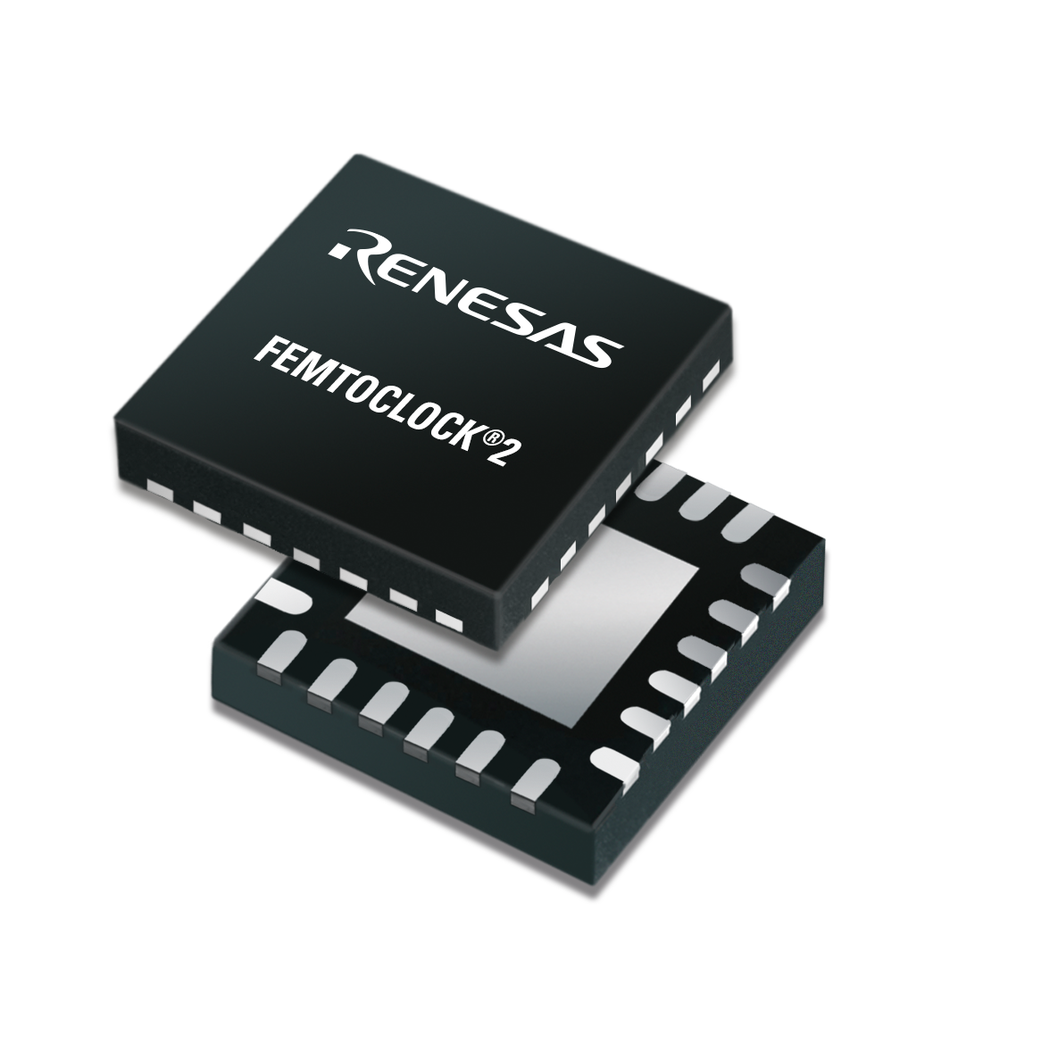
 Renesas Electronics Corporation expanded its timing solutions portfolio with a new sub-100fs point-of-use clock solution for data center, server, and network infrastructure markets. The new FemtoClock2 family includes ultra-low jitter clock generators and jitter attenuators in a small 4×4 mm2 package, enabling cost-effective and simple clock tree implementation for next-generation, high-speed interconnect designs.
Featuring best-in-class jitter as low as 64fs RMS, FemtoClock2 enables customers to easily meet next-generation PAM4 requirements on new switch or router designs. With a 4×4 mm2 form factor, the FemtoClock2 family is less than one-third the size of similar solutions on the market. This allows designers to place the clock source at the point of use – very close to the device receiving the clock signal – for streamlined PCB layout design, reduced cross talk, and cleaner signals. Flexibility makes the family useful in many applications. FemtoClock2 can be configured as a DCO, clock generator, or jitter attenuator, offering valuable design flexibility and reuse.
Key Features of the FemtoClock2 Family include: As low as 64fs (typ) RMS jitter; Low power consumption of 600mW; 4×4 mm2 in 24- and 28-pin QFN packages; Single & dual input options with four differential outputs; Power supply noise rejection better than -80dB; Output-to-output isolation of -80dBc; Compliant with ITU-T G.8262 and G.8262.1 for enhanced synchronous Ethernet/OTN; Integrated crystal option for more space savings;
Customers can combine the new FemtoClock2 solution with Renesas’ small, single-output, high-performance oscillators, or the broader ClockMatrix portfolio of timing solutions to address challenging timing needs for their high-performance server and network infrastructure designs. FemtoClock2 also works seamlessly with systems using the recently introduced PTP Clock Manager software for IEEE 1588 support and can be combined with Renesas’ complementary power and microcontroller offerings to create comprehensive solutions for a variety of applications, such as the IEEE 1588 Winning Combination. FemtoClock2 also serves as the downstream clock capable of delivering 100fs at the pin without disrupting the synchronization.
As the market leader in silicon timing, Renesas offers the only “one-stop-shop” for timing solutions, offering expertise and products from full-featured system solutions to simple clock tree building-block devices.
The RC32504A and RC22504A FemtoClock solutions and an evaluation board are available now. For more information, please visit renesas.com/femtoclock2.

Leave a Reply