Field programmable gate arrays (FPGAs) are digital ICs consisting of arrays of logic blocks that can be programmed (wired) and reprogrammed multiple times, even after the product containing the FPGA has been shipped and is “in the field.” FPGAs are not a monolithic technology; there are variations in how FPGAs are structured and programmed, variations in packaging, varying levels in integration, etc. And, FPGAs are not the only programmable logic devices available to designers. This FAQ will consider various FPGA embodiments and compare FPGAs with other programmable digital ICs. Subsequent FAQs will consider application factors when selecting FPGAs, how FPGAs’ use impacts the design process, and system integration challenges when using FPGAs.
An FPGA consists of an array of logic blocks surrounded by programmable input/output (I/O) blocks, with an overlay of programmable interconnects. There are several sub-architectures of FPGAs, some of which are discussed below. Optimization of FPGA performance in any specific application depends on selecting the correct device with the needed logic blocks, in an efficient architecture, and the optimization of the interconnect routing.
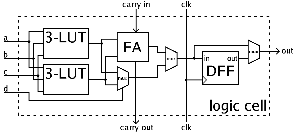
Compared with other programmable logic devices, such as simple programmable logic devices and complex programmable logic devices (both discussed below), FPGAs offer the highest logic capacity and performance. A typical FPGA can contain tens of thousands of logic blocks and an equally large number of flip-flops. FPGAs can be distinguished based on several factors, such as the relative size of the logic blocks they are composed of and the varying interconnect technologies used.
FPGA logic architectures
There are two primary classes of FPGA logic architectures, coarse-grained and fine-grained. Each architecture is suited for different classes of applications. The large logic blocks in coarse-grained FPGAs are typically composed of two or more look-up tables and two or more flip-flops. These FPGAs often include a four-input loop-up table that performs the logic functions. Coarse-grained FPGAs trade-off higher performance for specific functions than fine-grained implementations, but coarse-grained implementations are less flexible. Coarse-grained FPGAs are generally optimized for certain classes of applications, such as those requiring a large amount of floating-point computation.
Fine-grained FPGAs have a large number of simple logic blocks, usually containing either a two-input logic function or a 4-to-1 multiplexer and a flip-flop. These devices are good for performing systolic logic where the programmable interconnects can handle the processing dependencies and where the highly parallel data flow does not require sequential management. Systolic arrays (and FPGAs) are useful for applications such as artificial intelligence, image processing, pattern recognition, and so on.
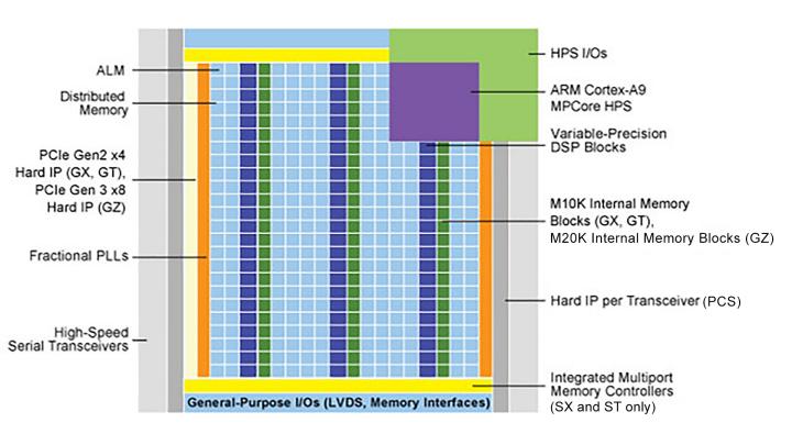
Many of today’s FPGAs combine coarse-grained elements within fine-grained programmable fabrics. The coarse-grained elements are also called “hard blocks”. They can include functions ranging from multipliers, high-speed I/O, and embedded memories to gigabit transceivers, complete DSP blocks, and embedded ARM processors. These hard blocks are separate from the programmable fabric and can provide ASIC-level performance and efficiency without occupying fabric resources, leaving the FPGA fabric available for application-specific functions.
Programming and interconnects for FPGAs
There are differences in the process technologies used to fabricate FPGAs in addition to differences between fine- and coarse-grained logic architectures. Most FPGAs use either static memory (SRAM) or anti-fuse CMOS technology. SRAM-based FPGAs are in-system programmable, whereas anti-fuse-based FPGAs are one-time programmable. SRAM-based FPGAs are generally higher density devices, while anti-fuse devices typically contain more plentiful programmable interconnect densities.
SRAM FPGAs are reprogrammable in the field after the system has been shipped but require an external configuration memory source. Anti-fuse FPGAs do not need an external configuration memory. The configuration memory used with SRAM devices contains the wiring program defining how all the FPGA elements are interconnected. Upon startup, the FPGA can load its configuration memory, or an external processor can load it. The configuration time is usually under 200ms.
Anti-fuse FPGAs maintain their program when the power is off, but they can only be programmed once. Programming of both SRAM and anti-fuse devices can be performed by the FPGA maker, a distributor, or the system maker.
3D packaging and heterogeneous FPGAs
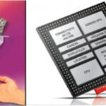
To continue shrinking the size and power consumption of advanced FPGAs, makers have adopted 3-dimensional (3D) or stacked architectures. There are two general approaches taken when packaging multiple die and FPGAs. In one case, several FPGA dies are packaged on a single piece of silicon that provides interconnects between the die. Multi-die construction enables different process technologies to fabricate specific parts of the FPGA to optimize overall performance. FPGAs consisting of multiple dies are called heterogeneous FPGAs.

Developments in 3D integration and packaging enable the complex system in package (SiP) implementations composed of multiple IC technologies that can help overcome Moore’s law limitations. The limitations of power, cost, and interconnects have been surmounted through innovations in stacking technologies that enable the fabrication and packaging of homogeneous and heterogeneous 3D ICs. These new SiP technologies can support emerging high-performance system requirements for very high interconnect bandwidth and minimal power consumption per bit.
Simple programmable logic devices
As their name implies, simple programmable logic devices (SPLDs) are small and simple programmable devices. They are the simplest form of programmable logic devices and are known by numerous names, including generic array logic (GAL), programmable logic array (PLA), and programmable array logic (PAL). While they are simple, SPLDs are highly flexible and are commonly used to replace logic components such as 7400-series TTL devices.
SPLDs are composed of a series of up to 24 macrocells that contain a combination of logic functions such as AND and OR gates and a flip-flop. Each microcell can perform a simple Boolean logic equation, which can be stored in the flip-flop, if necessary, until the next clock cycle. Like FPGAs, SPLDs can use fuses or various types of non-volatile memory cells to define the functionality. SPLDs have several advantages over 7400-series devices:
- A single SPLD needs less power, simpler wiring, and consumes less board space compared with the several 7400 devices that it replaces.
- SPLDs are flexible (and can be reprogrammable), so updating or changing the logic does not require changes to the circuit board. And it is also possible to replace one SPLD with another one programmed to a different design to change the logic.
- SPLDs can be used for various functions such as device-to-device interfaces, signal processing, decoding, data display, and timing and control operations.
Complex programmable logic devices
While much more complex than SPLDs, complex programmable logic devices (CPLDs) generally have far less processing capacity than FPGAs and are built using different architectures. The structure of CPLDs is not as flexible as FPGAs, with a few logic arrays feeding a relatively small number of clocked registers. But, CPLDs have more predictable timing delays and usually a denser logic-do-interconnect structure. CPLDs are dominated by logic, while FPGAs are dominated by interconnect.

FPGAs are more flexible but are more complex to design with, and FPGAs tend to be larger than CPLDs. FPGAs often include complex embedded functions such as memories, serializers/deserializers, analog front-ends, etc. CPLDs almost always have embedded flash to store their configuration, which is not usually the case for FPGAs. FPGAs require external non-volatile memory to store their programming.
Systems that require the logic to be already configured upon start-up generally use CPLDs. CPLDs and FPGAs can also be used in the same system. The CPLD(s) perform glue logic functions and boot up the FPGA and can be used to control the boot and reset functions for the overall system, while the FPGA(s) perform all the heavy processing functions.
Application specific integrated circuits
FPGAs also compete with application-specific ICs (ASICs) and application-specific standard parts (ASSPs). A system that previously needed multiple ASICs and/or ASSPs can now use a single FPGA. Compared with multi-chip solutions, a single FPGA can offer reduced power needs, increased speed, less board space, and the possibility for reconfiguration even after the product has shipped.
ASICs and ASSPs can provide benefits over FPGAs in some applications. In high-volume applications, ASICs and ASSPs can cost less than FPGAs. Some designers use FPGAs during product development to take advantage of their flexibility during design iterations, moving the final design into an ASIC, so it cannot be modified after the design has been finalized, improving system security.
Another product category is FPGAs embedded in ASICs. Called eFPGAs, these devices combine the security benefits of ASICs with some of the flexibility of FPGAs. eFPGAs can be scalable to meet specific application needs. And eFPGAs can be used to extend ASIC lifetimes by providing programmability for functions such as algorithms and protocols that can evolve over the system’s life.
FPGAs are the most complex digital ICs that are reprogrammable. ASICs and ASSPs can be more complex than FPGAs but are not reprogrammable. SPLDs and CPLDs are reprogrammable but are much less complex compared with FPGAs. FPGAs are being used in more and more applications due to their high-performance capabilities and programmability. The next FAQ in this series will look into the application considerations when selecting FPGAs.
References
3D ICs, Xilinx
Application-specific integrated circuit, Wikipedia
Enabling Next-Generation Platforms Using Intel’s 3D System-in-Package Technology, Intel
Programmable logic device design guidelines, Microchip

Leave a Reply