The high level of integration in today’s mmWave phone means traditional test methods no longer apply.
5G, the first cellular generation to use the mmWave spectrum, can deliver faster data rates (up to 10x better than LTE). Plus, 5G can accommodate more simultaneous subscribers with higher reliability services. These improvements make 5G ideal for specific deployments such as dense urban environments — airports, stadiums, and metropolitan areas.
mmWave smartphones contain highly integrated components. Unlike at lower frequencies, test systems can no longer perform conducted tests at all manufacturing steps. While testing at the wafer level can use techniques found at sub-6 GHz frequencies, mmWave components such as antenna-in-package (AiP) must use over-the-air (OTA) test procedures.
Why mmWave?
In the US, the network operators have procured mmWave bands and deployed mmWave networks. Table 1 outlines the four primary mmWave bands (i.e., 24 GHz, 28 GHz, 39 GHz, and 47 GHz) by carrier.
|
||||||||
| Table 1. U.S. carriers and their mmWave frequency bands. |
According to a mobile data traffic outlook report from Ericsson, the typical US subscriber in 2028 will consume 55 GB monthly. Why so much compared to today’s roughly 15 GB averages? This predicted traffic growth comes from estimates for extended reality-type services (XR) — augmented reality (AR), virtual reality (VR), and mixed reality (MR). On top of that, increased and higher-resolution video traffic, currently about 70% of all data traffic, will also contribute to this growth.
mmWave hasn’t yet seen the accelerated growth that typically accompanies new connectivity technologies. The data-traffic outlooks indicate that it won’t be long before congestion and hunger for throughput open the floodgates. The initial generation of mmWave-capable devices will help develop the mmWave ecosystem, which includes manufacturing tests.
While the US has allocated 39 GHz and 47 GHz for cellular use, the 26 GHz to 28 GHz mmWave band seems poised to become the standard for global coverage. Therefore, we expect the target market for mmWave will soon become ten times larger, measured in billions of subscribers.
Forward-looking manufacturers have risen to meet this emerging demand. Since 2019, more than 400 5G mmWave capable mobile devices have come to market, which indicates that mmWave is catching on. Table 2 breaks down these device capabilities according to their supported mmWave bands.
|
||||||||||
| Table 2. Mobile devices capable of accessing 5G mmWave technology arranged by band. |
Now that we’ve seen things from the network operators’ perspective, these smartphones are worth a closer look to understand the other half of the wireless equation.
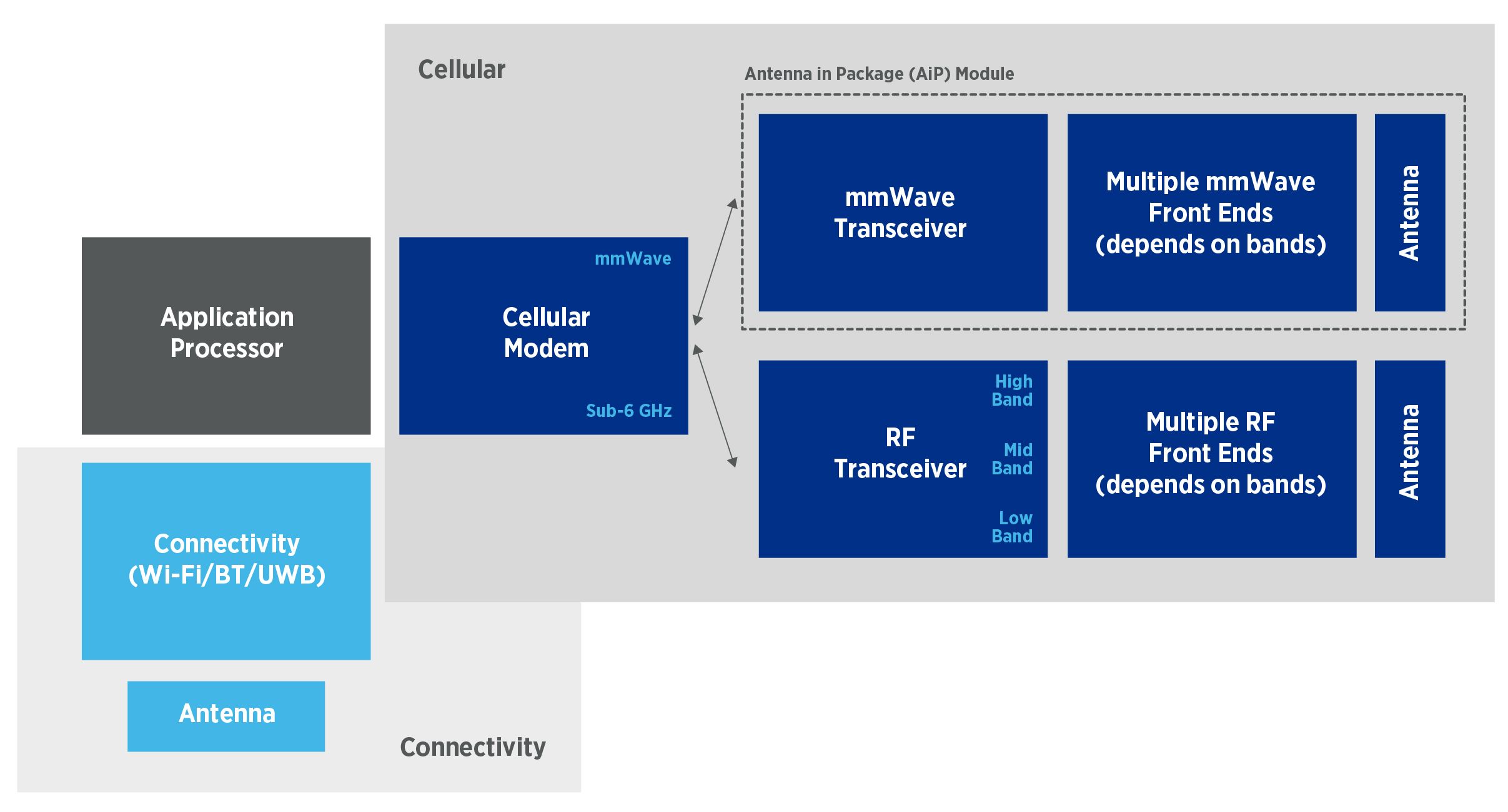
Figure 1. This functional block diagram shows basic 5G smartphone components, with the cellular modem supporting both traditional RF (sub-6 GHz) and mmWave signal chains.
Inside today’s 5G smartphone
The functional block diagram in Figure 1 shows how 5G smartphones organizes the intricate constellation of components to enable wireless communication between subscribers and network operators. The application processor, which controls all
smartphone operations, joins everything. In general, the connectivity bands are served by separate RF signal paths for unlicensed band operations such as in the 2.4 GHz, 5 GHz, and 6 GHz bands. Similarly, separate RF and mmWave paths serve licensed-band operations for the cellular bands.
Think of each wireless signal path as consisting of a modem,
transceiver, and path to an antenna(s), which could include
other RF front-end components such as switches, tuners, and
multiplexers. In this organized manner, the wireless signal
paths between the application processor and the antennas become
the many pathways from RF to bits. And these paths establish the
wireless links that deliver wireless services for the
subscriber.
Focusing on the cellular path, the modem is the hub for the
wireless cellular linkages. Furthermore, the RF transceiver
handles all the sub-6 GHz activities for data transmission and
reception. Likewise, the mmWave transceiver handles all mmWave
data transmission and reception. The actual number of wireless
bands depends on the network operator’s plan to deliver services
to their subscribers.
RF and mmWave transceivers
The RF transceiver must support all operational bands for the network operator. Within the transceiver are separate transmit and receive paths for each band. The total number of bands depends on a network operator’s spread across 1G/2G/3G/4G/5G and could total as many as 70 bands. Additionally, antenna technology has evolved to accommodate massive input, and massive output (MIMO) features that simultaneously transmit and receive on four antennas. Thus, the transceiver must perform consistently at high levels and across all supported bands. This vital functionality, flexibility, and reliability rest on remarkable integration and complexity that needs testing.
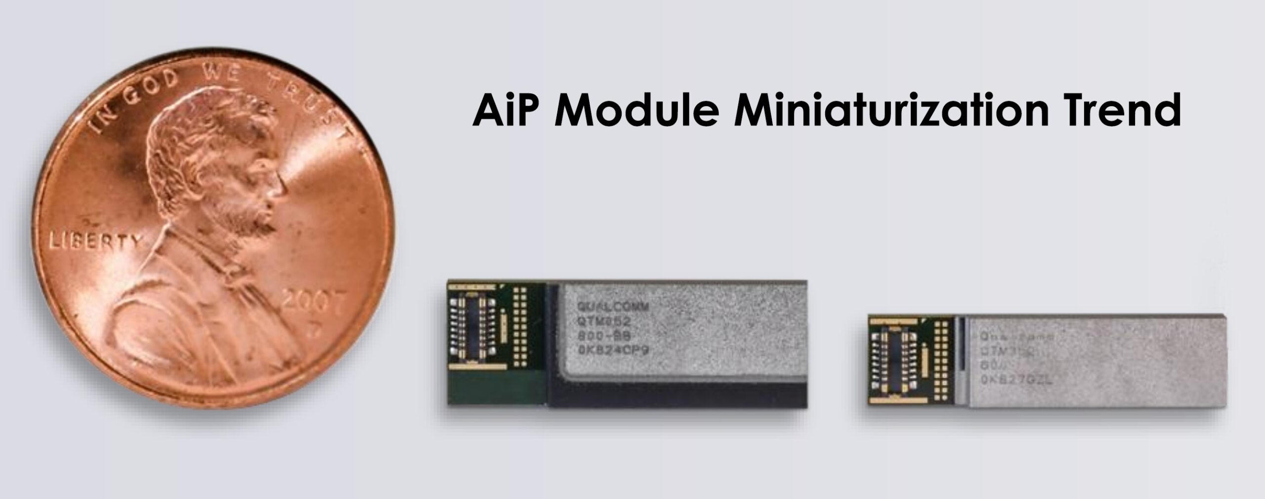
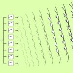
Figure 2. AiP module view from Qualcomm showing miniaturization trend in package size.
Like the RF transceiver, the mmWave transceiver must also support all of a network operator’s operational bands. In the mmWave spectrum, these bands are the 24 GHz, 28 GHz, 39 GHz, and eventually, 47 GHz bands. Given that mmWave communication involves shorter wavelengths relative to sub-6 GHz, its signal paths are also smaller. In fact, the semiconductor ecosystem seems to have standardized on an antenna in package (AiP) module to combine the mmWave transceiver, power management IC (PMIC), beamformer, and antenna array into a single modular package. Figure 2 illustrates this miniaturization trend by showing AiP modules, where the most modern is at right. This makes the AiP module easy to integrate into a signal path but makes testing them more difficult.
As Table 3 summarizes, AiP has undergone four generations so far. The current AiP modules support multiple mmWave bands. This achievement has accelerated mmWave technology adoption. It also shows how additional band support has an inevitable ripple effect because all the signal paths must align to support the wireless link.
| AiP Evolution | 1st gen (2018) | 2nd gen (2019) | 3rd gen (2020) | 4th gen (2021) |
| Qualcomm’s generations | QTM052 5 Gb/sec for X50 modem Bands n257, n260, n261 |
QTM525 7.5 Gb/sec for X55 modem Adds band n258 |
QTM535 7.5 Gb/sec for X60 modem Adds sub-6 GHz carrier aggregation |
QTM545 10 Gb/sec for X65 modem Ads band n259 (not n262, 47 GHz yet) |
Table 3. Qualcomm’s AiP modules keep adding bands and increasing data rates as each successive modem hits the market.
We can now see how the application processor, cellular modem, and transceivers have become integrated, complex semiconductor devices. Even this virtual tear-down risks oversimplification. Many of these devices have separate PMICs that regulate their power to improve battery life. They also contain custom antennas that streamline the signal paths to the base station with highly optimized signal-to-noise ratios to achieve faster and more reliable data rates.
Implications for automated test
As we’ve seen, the main functional blocks of a 5G smartphone include the application processor, modem, transceiver, RF front end, and antenna. Every successive generation of these devices has ripple effects in the advanced packaging necessary to achieve higher performance and more complex integration. Automated test equipment (ATE) Satisfies the production need for quality.
Test workflow for high-volume manufacture of Sub-6 GHz components has become ubiquitous. Test engineers attempt to eliminate defects as early in the production process as possible. As a rule of thumb, defects get ten times more expensive to capture at each successive production step.
The wafer test insertion uses ATE to separate good and bad die. These tests are usually electrical in nature (not RF). This first test insertion, termed wafer sort, is designed to eliminate as many defects as possible. As a result, this step typically has the lowest yield.
Next, package-level test also uses ATE to ensure operation and performance that meets statistical expectations to avoid shipping defects and outliers. These RF tests consist of both CW and modulated signals and can include calibration procedures. This insertion is designed to typically have a much better yield than the wafer test.
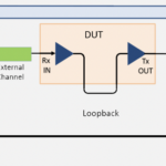
Lastly, the RF chip integrates into a module (or system assembly) to finalize the RF signal chain and fulfill its mission in the smartphone architecture, including antenna connection(s). In this production step, the module undergoes one last system-level test (SLT) insertion for a conducted test (not over the air, OTA), including possible calibration procedures. This insertion typically provides the highest possible yield.
This workflow ensures quality and consistency throughout the supply chain for the RF signal chain, whether this package serves a singular function or offers integrated capabilities. Note that test coverage is the sum of all three insertions and variations on the test strategy are possible depending on the root cause of defect mechanisms. The manufacturing goal is defect-free shipments. In practice, the quality metric describing the final SLT output is measured by defective parts per million (DPPM).
This Sub-6 GHz workflow also represents the best practices to follow for manufacturing the AiP module in the mmWave signal chain.
Advanced packaging in the AiP module enables miniaturization within the 5G smartphone. It also imposes on the manufacturing process, which must adapt to the complexity and integration of the mmWave signal chain into this single package. As we compare the RF and mmWave signal chains, two main differences summarize these mmWave test challenges for AiP modules.
- In the interest of miniaturization, the AiP module doesn’t employ the same traditional packaging techniques employed in the previously described RF workflow. Instead, advanced packaging to integrate die with substrate and antenna array introduces new challenges to finding defects related to the elimination of packaging elements to achieve miniaturization.
- Given the small wavelengths in mmWave, close coupling between the transceiver and antenna array (via a substrate) offers superior wireless performance compared to using separate, discrete elements. This tight coupling eliminates excessive transmission loss. Unfortunately, it also eliminates conventional test points and best practices for the conducted test. A new test method that measures differences between antenna array — over the air (OTA) and available conducted test interface at 5G-IF — is necessary for calibration and defect detection.
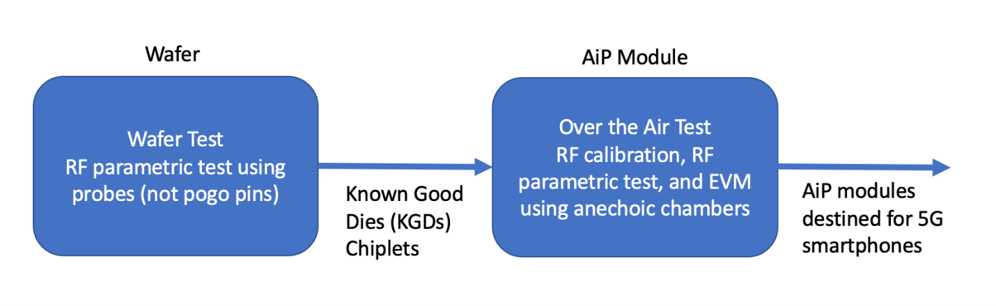
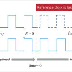
Figure 3. The mmWave workflow to uncover defects consists of wafer sorting using RF followed by a system-level test using OTA methods.
Compared to the RF best practices, the mmWave workflow illustration in Figure 3 shows the new emerging simplification and complexity in testing AiP modules.
Test workflow for high-volume manufacture of mmWave components has yet to become as ubiquitous as with RF. Indeed, it’s still evolving with every new generation of AiP modules. Like RF, test engineers attempt to eliminate defects as early in the production process as possible.
As with sub-6 GHz, wafer-test insertion uses ATE to separate good and bad die. These tests employ wafer probes and test with both electrical and mmWave signals. This first test insertion, termed wafer sort, eliminates as many defects as possible and, as with the RF test, typically has the lowest yield. The output is a known good die (KGD).
Lastly, the KGD integrates into the AiP module to finalize the mmWave signal chain. In this production step, the module is placed in an optimal anechoic chamber that is handler-friendly and undergoes one last system-level test (SLT) insertion using OTA methods, including possible calibration procedures using both CW and modulated signals. This insertion is designed to typically provide the highest possible yield.
Like the RF signal chain, this workflow ensures quality and consistency in the mmWave signal chain. Note that test coverage is the sum of all three insertions and variations on the test strategy are possible depending on the root cause of defect mechanisms.
Conclusion
With so many variables and technologies at play, testing the RF-to-bits components inside a 5G smartphone is no small task. Any test strategy for 5G smartphones must account for higher frequency, greater bandwidth, increased site density, and enhanced performance while also maintaining automated test equipment (ATE) expectations for modularity and versatility. This requires expertise in many disciplines to succeed, especially when that test leaves no room for manual intervention. If successful, however, it can fuel innovation, quality, and profitability by meeting manufacturing volumes and lowering test cost.