It is easy for developers to get tripped up when cramming multiple antennas into the small spaces that characterize IoT applications.
Rich Walters • Brian Petted, Laird Connectivity
Traditionally there has been a wall between industrial design and RF (radio frequency) engineering when companies develop products that have wireless capabilities. The process typically starts with product designers assembling a list of design requirements that determine the look, feel and function of the product. Only with the product development process well under way are RF engineers tasked with squeezing in wireless capabilities. Simply put, the wireless antenna and its performance can be afterthoughts.
The problem, of course, is that wireless products designed this way run the risk of underperforming and being impractical – perhaps forced to use off-the-shelf antennas inappropriate for the constrained location and proximity to perturbational materials. Stick-on antennas, for example, can be detuned by most plastics. Volume constraints introduced by prescribed industrial and mechanical designs often suggest the use of a “chip” antenna. However, many chip antennas require a printed circuit board (PCB) footprint and features that may not comply with the size constraints.
It is remarkable that many manufacturers don’t integrate the RF and industrial design teams to avoid making costly changes late in development. A well-integrated team can define early boundaries for the product that could simplify antenna design later. Moreover, designing the antenna and PCB layout without input or constraints from industrial designers can lead to missed opportunities for optimizing the shape, performance, size, cost, assembly, and desirability of the product.
For example, it may not occur to RF designers operating alone that it could be advantageous to integrate antennas right into the product housing, essentially creating a Molded Interconnect Device (MID) — basically, injection-molded plastic with integrated circuit traces. The MID can be an internal part or integrated into the exterior of the product. There are several ways to produce MIDs and some of them require less tooling than others.
This sort of design thinking takes a team of industrial designers and antenna designers who work side by side, simulating antenna patterns, building prototypes, and testing real physical prototypes. In this scenario, RF engineers make sure industrial designers know about limitations as well as spatial and material challenges for the chosen antennae. They can also factor in spatial and material limitations such as those imposed by adjacent ground and dielectric planes, human body interactions, and resistive loss characteristics of metallization materials and processes.
Antenna design
Products ranging from smartphones to the PlayStation 4 all contain at least one antenna comprised of a printed circuit board trace. A trace antenna has several advantages. Good performance, virtually no additional cost, and small size for frequencies exceeding 900 MHz are some of the reasons trace antennas are popular.
There are several factors helpful to keep in mind when implementing a trace antenna. Standard printed or trace antenna designs that are widely used include various monopoles, dipoles, loops, notches, slots, and PIFAs (planar inverted-F antennas). Standard PIFA-type antennas are the most extensive and offer the best trade-off between size, efficiency, and are reasonably omnidirectional. A meandering trace can be used to compact the PCB area but at the cost of performance.
Of course, the PCB trace length determines the antenna resonant frequency. Each antenna requires a keep-out area around the antenna trace where no copper traces or ground fill can exist on any layer of the PCB. The trace can either be gold flashed or covered with solder mask. The antenna’s electrical performance will be determined by the type of substrate material, its thickness, relative dielectric constant (εR), and metallization resistivity.
Most non-dipole PCB trace antennas must have an image ground plane to be effective. The shape and size of the ground plane relative to the antenna affects the antenna impedance and performance. The ground plane should have vias along the entire edge of the antenna keep-out area to connect ground planes in multi-layer designs.
A mismatched antenna can greatly reduce the total RF link budget and range due to mismatch losses, therefore the addition of a matching network at the antenna feed point is a best practice. Additionally, the final tuning and matching should take place in the actual product enclosure, not in open air. Maximum RF power transfers when the antenna impedance matches the source impedance (usually 50 Ω). Ideally, a return loss below -9 dB or 2.0:1 voltage-standing-wave-ratio (VSWR) is often taken as a figure of merit for a good antenna match, which translates to 12.6% of the incident power reflected due to mismatch. For band-edge frequencies, a degradation of return loss from -9 to -6 dB (25% reflection of incident power) is conventionally accepted.
Plastic enclosures, metal components, and the presence of other components close to the antenna all affect the antenna tuning and radiation pattern. Avoid placing the antenna close to metallic objects, nor enclose the antenna in a metallic or metalized plastic enclosure. Ideally, keep external influences in the antenna far field.
All PCB antennas are on the dimensioning of the lateral and vertical geometries of antenna element patterns as well as the electrical parameters that make up the structure of the specific design. This implies that the simple copying and translation of an existing design probably won’t work well without adjustments. Gain and radiation patterns will vary as the dimensioning and material properties in the surrounding areas change. The length of the antenna will typically require adjustment in response to these variations.
Diversity antenna array placements create a challenge in that one must place and orient independent antennas such that each antenna’s pattern does not couple to the same space as the other (patterns are not correlated to a common phase center). This is true for Selection Diversity (select antenna with best signal) as well as Multiple-Input-Multiple-Output (MIMO) antenna systems.
Typical methods of reducing antenna pattern correlation create space between the elements (up to a quarter wavelength) or create an orthogonal (90°) relative orientation (or both). Compaction of these array placements requires close attention not to degrade the diversity gain performance of the system.
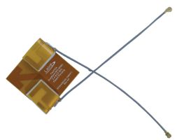
There exist dual-element sub-arrayed antennas to simplify the compaction and placement process. Examples include the world’s first flexible PIFA (planar inverted F antenna) for Wi-Fi MIMO applications (patent pending). The FlexPIFA MIMO is specifically designed for 802.11 a/b/g/n as well as 802.11ac Wi-Fi modules that use MIMO or Wi-Fi Diversity. The Laird FlexPIFA MIMO drastically simplifies the size, cost and technical requirements for implementing the two antennas necessary for 802.11 MIMO because the two integrated antenna elements are oriented and spaced in an optimum way for MIMO radio performance.
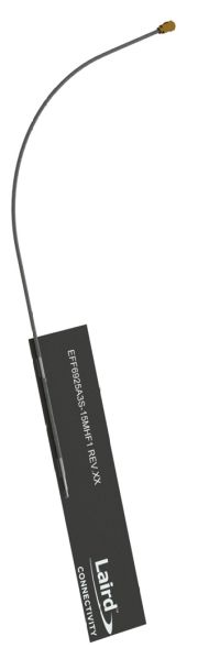
Some antennas are purposely designed to be placed in direct contact with particular packaging materials. These antennae usually are slot type or post-loaded dipoles. An example of these types of antennae are the FlexNotch and Mini NanoBlade Flex. Another notable flexible antenna is the Revie Flex for use in LTE CAT M1 and NB-IoT devices. The antenna is optimized for mounting to plastic via a supplied adhesive backing. It operates within the 698 – 875 MHz and 1.71 – 2.5 GHz bands and is ground-plane independent.
Certifications and compliance
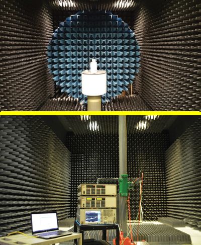
Radio regulatory certification is a critical step in every wireless product launch, but obtaining it isn’t always straightforward. Successful navigation of the FCC certification landscape is critical for getting to market quickly. Pre-scans are an effective way to reduce the risk of failing – basically, checking the product for emissions while still in development.
Unfortunately, many teams get to the final stage of development before thinking about regulatory testing. Products can fail regulatory certification on the first test attempt and in light of empirical experience, wireless products with embedded radios are even more likely to exceed regulatory limits, problematic because resolution of these failures typically requires last-minute hardware changes.
The integration of antennas within the packaging dictated by product form and function should be a team effort between RF engineering and Industrial-Mechanical design. Common considerations amongst the co-development team should be harmony with the industrial and mechanical design, while maintaining a firm observation of best-practices for antenna placement and implementation for radio performance and success of regulatory testing and compliance. This effort can be synthesized from raw materials and design know-how or can be implemented with off-the-shelf solutions that reduce design risk and cycle-time.
Leave a Reply