The number of internal memories in an MCU depends on how the memory is categorized. At the highest level, there are two; random access memory (RAM) and read-only memory (ROM). But, if the interest is in memory performance, there are different types of RAM and ROM. And these different types of memory can be employed for various functions such as cache memory, main memory, program memory, and so on. On the other hand, there’s the question of virtual versus physical definitions of memory.
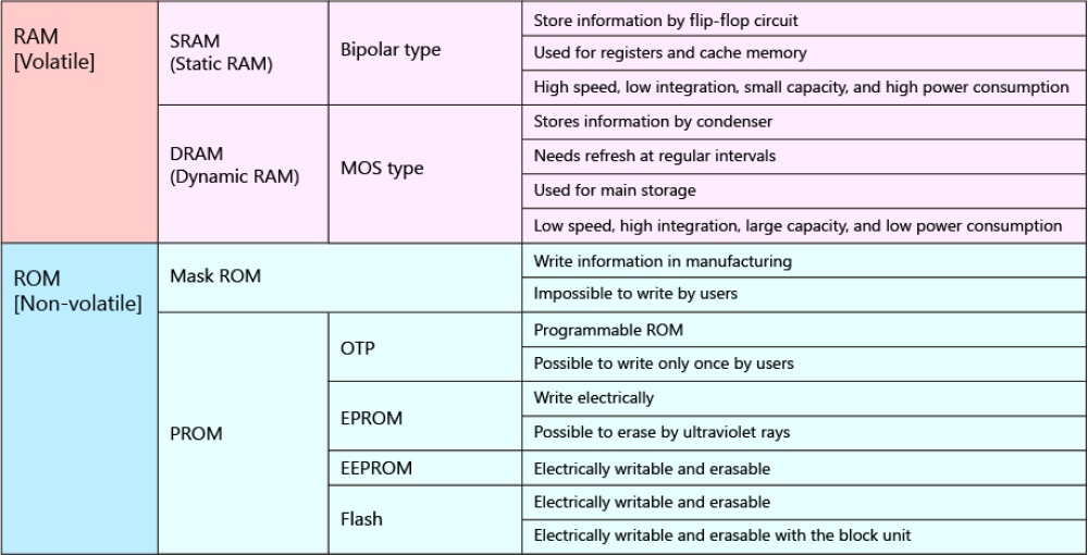
The two primary types of RAM are static random-access memory (SRAM) and dynamic random-access memory (DRAM). Both need voltage applied to hold their information. DRAM is simple and requires only one transistor and one capacitor for a basic implementation. DRAM is the most widely used of all memory technologies. When integrated into an MCU, it’s called embedded DRAM (eDRAM). The cost-per-bit for eDRAM is higher when compared to equivalent standalone DRAM chips used as external memory. Still, the performance advantages of placing eDRAM onto the same chip as the processor outweigh the cost disadvantages in high-performance applications.
SRAM is more complex than eDRAM and is usually implemented with six transistors in CMOS. SRAM is also faster than DRAM, making it highly suitable for integration into MCUs. It’s one of the most-used internal MCU memory technologies. SRAM is commonly used as the cache memory and for processor registers.
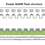
Nonvolatile memories in MCUs include Flash and electrically erasable and programmable ROM (EEPROM). Flash memory is a form of EEPROM. The primary difference between them is how they are managed; Flash is managed (written or erased) at the block level, and EEPROM can be managed at the byte level. Flash memory is available in NAND and NOR architectures. NAND Flash handles data in blocks and reads faster than it writes. It can quickly transfer while pages of data. It offers higher capacity per unit area than NOR and is used for high-density storage. NOR Flash supports more granular operation, and it provides high-speed random access. NOR Flash can read and write data in specific
Fujio Masuoka invented Flash memory when he worked for Toshiba in the 1980s. His colleague, Shoji Ariizumi, used the term Flash to describe the new technology because erasing all the data reminded him of the Flash of a camera. Volatile and non-volatile memory technologies can be compared based on several performance criteria (Table 1):
- Speed: Volatile memory is generally faster
- Cost: Volatile memory costs less
- Lifetime: Volatile memory has a longer lifetime. Non-volatile memory has a limited lifetime due to its re-write capabilities.
- Energy consumption: Volatile memory such as DRAM requires repeated data refreshes, which consume additional power. Non-volatile memory generally consumes less power.
Memory hierarchies
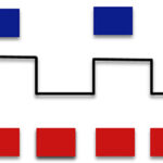
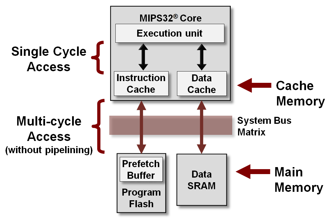
The cache memory is a critical system in an MCU. There are two ways to categorize cache memory: a hierarchy or functionality. When described in terms of a hierarchy, there can be up to 4 levels of cache memory. The cache consists of fast memory, such as SRAM and eDRAM to compensate for the slower access time of the main Flash memory. A Level 1 cache is a small block of memory that can run as fast as the CPU to support maximum processing speed. Level 2 and Level 3 caches support the Level 1 cache. They are larger and slower than the Level 1 cache but have faster access times than the main memory (Figure 1).
In terms of performance and size, eDRAM sits between level 3 cache and conventional DRAM on the memory bus and functions as a level 4 cache. The higher density of eDRAM compared with SRAM can support much wider buses and higher operating speeds. And larger amounts of eDRAM can be integrated into a smaller area than SRAM. It’s more complex to fabricate eDRAM than SRAM, but the 3x area savings with eDRAM can offset the fabrication costs when large amounts of memory are needed.
For any given level of cache memory, all blocks have the same size and associativity. Lower levels like Level 1 cache have fewer blocks, smaller block sizes, and fewer blocks in a set, but they provide very fast access times. As the Level increase to 2 and 3, cache memory has an increasing number of blocks, larger block sizes, and more blocks in a set. But every level of cache memory is much faster than the main memory. In addition to the main cache memory, specialized types are used for specific functions. Examples include:
Pipeline cache. Pipelined CPUs, for example, in RISC MCUs, access memory from multiple points in the pipeline, including data fetch instruction fetch and virtual-to-physical address translation. The pipeline uses three specialized caches: data, instruction, and translation lookaside buffer (TLB).
Victim cache. Blocks of data that have been replaced and deleted from a CPU cache are held in the victim cache. The victim cache sets between the main cache and the refill path. It’s fully associative and is designed to reduce the number of conflicts misses in programs that can benefit from a highly associative mapping. In some implementations, Level 4 cache can function as a victim cache.
Micro-operation (μop) cache. This cache stores micro-operations of decoded instructions received from the instruction cache or the instruction decoder. It can speed processing. The μop cache is checked when an instruction needs decoding to see if its decoded form is already available. If it’s unavailable in the μop cache, the instruction is decoded and cached for future use.
Memory organization and MCU architecture
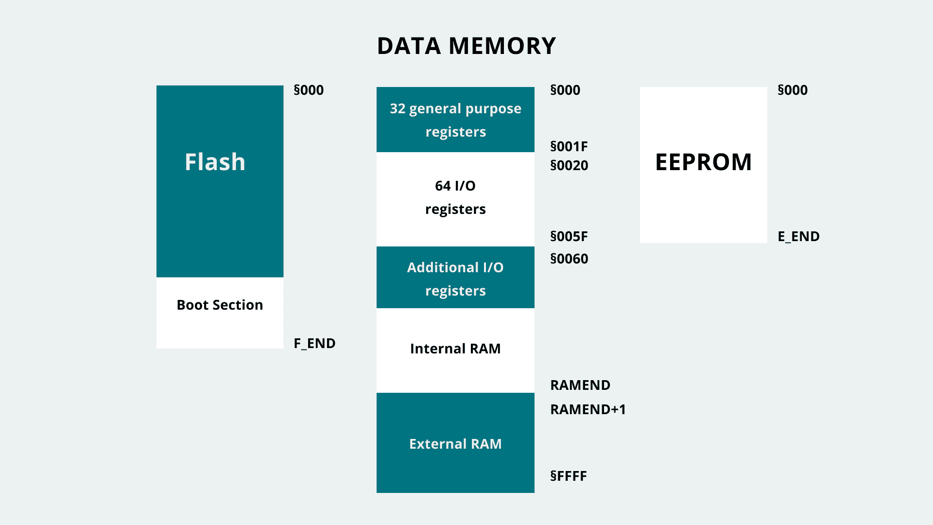
Different MCU types, such as the AVR and ARM architecture, use different ways to organize memory. The Harvard-based AVR architecture organizes memory into Flash, internal and external DRAM, and EEPROM (Figure 2). As a result, systems using these MCUs organize the memory into specific sections, including:
- Text
- Data
- BSS
- Stack
- Heap
The text section contains instructions loaded into the Flash memory; data section contains variables that have been initialized, the BSS contains uninitialized data, the stack includes data of functions and interrupts, and the heap contains variables created during run time.
In ARM MCUs, memory maps are used with a different address configuration of 32-, 36-, and 40-bits that depends on the requirement of system address space and extra DRAM. A memory management unit (MMU) controls memory access instructions that can be used on high-level code to manage interrupt modules and integrated peripherals.
The primary purpose of the MMU is to enable the processor to run multiple tasks independently in a virtual memory space. The MMU uses translation tables to bridge virtual and physical memory addresses. Virtual addresses are managed through software with memory instructions. Physical addresses are controlled based on a translation table input given by the virtual address (Figure 3).
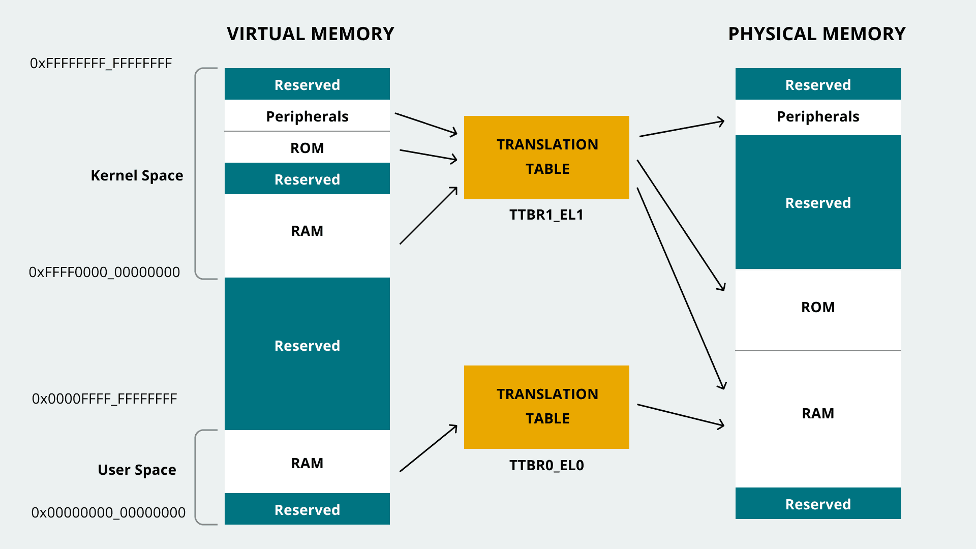
The MMU is a specialized memory unit and includes the table walk unit that reads the translation tables from memory and TLBs, which cache recently used translations. All memory addresses from the CPU software are virtual. The MMU checks the TLBs for a recently cached translation. If one doesn’t exist, the table walk unit reads the appropriate table entry, or entries, from memory
Summary
MCUs include various forms of RAM and ROM to support specific performance requirements. The most common forms of memory in MCUs include eDRAM and SRAM volatile memories and Flash and EEPROM non-volatile memories. Flash and EEPROM are generally used for the main memory, while eDRAM and SRAM are used for various cache memory functions. In addition, MCU memories are organized based on virtual and physical addresses and functionality and are managed with an MMU.
References
Arduino Memory Guide, Arduino
CPU Cache, Wikipedia
Memory Architectures, Adafruit
Memory Type (RAM & ROM), Toshiba Electronic Devices, and Storage
What is cache memory?, Microchip