Lattice Semiconductor Corporation announced its new low power FFPGA platform, Lattice Nexus. The platform is architected to deliver power-efficient performance that will benefit developers of a wide range of applications, including AI for IoT, video, hardware security, embedded vision, 5G infrastructure, and industrial/automotive automation. Lattice Nexus is built with innovations at every level of design, from solutions, to architecture, to circuit, and delivers higher system performance at significantly reduced power consumption.
To increase ease-of-use for customers, the Lattice Nexus platform provides innovative system-level solutions that combine design software and pre-engineered soft IP blocks with evaluation boards, kits and reference designs to enable them to build their systems more quickly. These solutions target key growth application areas like embedded vision and include solutions like sensor bridging, sensor aggregation and image processing.
The Lattice Nexus platform has innovative architectural features that optimize system performance at industry-leading low power. For example, the platform’s optimized DSP blocks and higher on-chip memory capacity enable power-efficient computing, such as AI inferencing algorithms, and runs twice as fast at half the power of Lattice’s previous FPGAs.
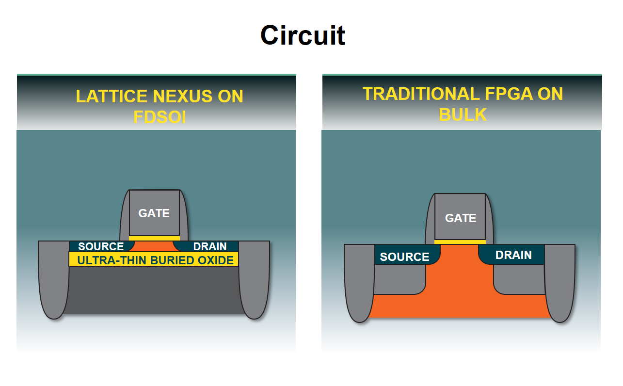
Lattice Nexus also uses innovative circuit design to deliver key capabilities to customers, including programmable power-performance optimization and very fast configuration for instant-on type applications.
Lattice Nexus is developed on high-volume 28 nm fully-depleted silicon-on-insulator (FD-SOI) process technology from Samsung. This innovative technology features 50 percent lower transistor leakage compared to bulk CMOS, and is the best technology for delivering the low power Lattice Nexus platform.
Leave a Reply