by Electro-Tech-Online member languer
In the past when requiring to monitor I2C communications between two devices I would use a logic analyzer. Such monitoring was useful to determine if the I2C communications between devices was properly configured. Even though this is quite useful and efficient, it does require a logic analyzer, with an I2C protocol debugger. Such devices are actually pretty common and not too expensive (e.g. Saleae Logic analyzer), but sometimes these may be overkill and a small specialized device may suffice. In comes the I2C monitor. Something which:
- can monitor simple I2C communications between two or more devices (at up to 100kHz bus speeds)
- does not respond, acknowledge, or in any way modify the communication being monitored
- outputs the transactions through RS232
This is nothing new. In fact the ideas behind this project were born from the following projects:
I2C Bus Sniffer on AVR
Robust I2C Slave Without a Sampling Clock
Design
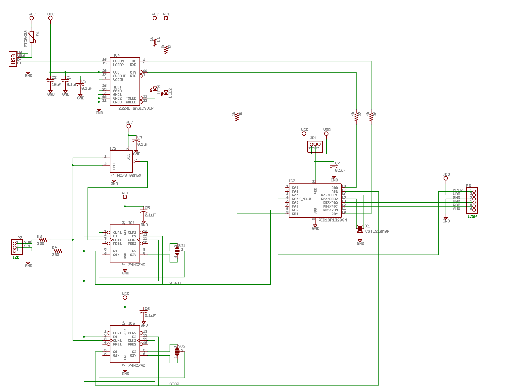
To monitor simple I2C communications between two or more devices and output these transactions through RS232 to a PC, in some of the reference designs listed before most of the work is done by the MCU. The MCU samples the SCL and SDA lines and has to determine the START and STOP conditions, as well as the normal data. The flow diagram sort of goes as follows:
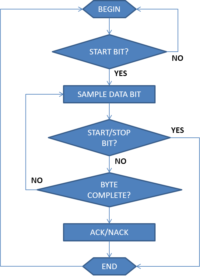
To help the MCU keep up with the data, external hardware is added to handle the Start and Stop conditions. This was done on both the “I2C Bus Sniffer on AVR” and “Robust I2C Slave Without a Sampling Clock” articles. Such implementation requires four dedicated pins: three interrupt pins (one for Start condition, one for Stop condition, one for SCL), and one standard input for SDA. In addition the MCU requires built-in USART hardware.
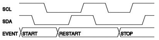
The next figure provide illustration of how create the two additional hardware blocks for the Start and Stop conditions needed. During normal transactions the SDA (data) line is only allowed to change when the SCL (clock) line is at a logic low. A Start and Stop condition is then defined by a change of the SDA line when the SCL line is at a logic high; the Start condition indicated when the SDA transfers from at a logic high to a at a logic low with the SCL at a logic high, and the Stop condition indicated when the SDA transfers from at a logic low to a at a logic high with the SCL at a logic high.
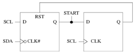
Flip-Flops can be used to create a simple method to identify these conditions, and create simple pulses to indicate either condition. The next figure shows a dual D-type flip-flop configuration used to determine a Start condition.
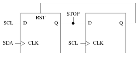
The following figure, on the other hand, shows a dual D-type flip-flop configuration used to determine the Stop condition.
These Flip-Flop hardware blocks together with the MCU can now provide the building blocks for the I2C monitor. The I2C Start command, as decoded by the flip-flop, can trigger an I/O interrupt on the MCU indicating the start of the message. The I2C Stop command, as decoded by the flip-flop, can trigger a separate I/O interrupt on the MCU indicating the end of the message.
For proper operation, the following requirements exist for the MCU:
- MCU must be clocked at the highest MHz rate possible (this is to be able to keep up with high data rates during the interrupt routines)
- MCU requires dedicated USART hardware/pins
- MCU requires three interrupt pins
For the implementation Microchip’s 18F1320 PIC was chosen. This MCU has the following specifications:
- 40MHz clock (10MHz internal – using x4 PLL)
- Two dedicated USART pins
- Four dedicated interrupt pins (one is shared with USART, so CCP pin is used as third)
Implementation
The following figure shows the implementation of the proposed design. For a quick prototype, the FTDI interface was replaced with an FTDI TTL cable. Oshonsoft Basic was used to code and simulate the PIC MCU operation before actual implementation and testing of the hardware. The prototype worked as expected with two caveats: (1) the maximum bus supported speed is 100kHz, and (2) if the internal buffer on the MCU overflows there is currently no indication for this. Ideally such a device would work for I2C communications up to 400kHz, but this is limited by the PIC MCU clock and the RS232 output routines. The higher I2C communications are better suited for an FPGA implementation.
Click ASM Code for pdf of full Code
Can you explain what the jumpers SJ1 and SJ2 are for?