The Inter-Integrated Circuit (I2C) protocol has been the backbone of short-distance, intra-board communication. However, implementing robust I2C communication is not just about connecting two wires. This FAQ analyzes the open-drain physical layer and the nuances of register-level addressing to better understand I2C communication.
How does I2C differ from push-pull interfaces like SPI?
The defining characteristic of I2C is its open-drain (or open-collector) architecture. Unlike SPI or UART, which use push-pull drivers to actively drive lines HIGH and LOW, I2C devices can only drive the bus LOW. They cannot actively drive the bus HIGH.
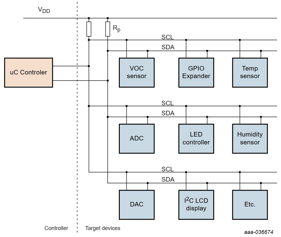
Figure 1 illustrates this topology. It shows multiple devices (Controllers and Targets) connected to the shared Serial Data (SDA) and Serial Clock (SCL) lines. Worth noting is that both lines are connected to the positive supply voltage (VDD) via external pull-up resistors (Rp).
The LOW and HIGH operations of I2C can be understood as follows:
- Logic 0 (LOW): To transmit a zero, an internal N-channel MOSFET within the device turns on, connecting the signal line directly to ground. This circuit actively sinks current.
- Logic 1 (HIGH): To transmit a one, the device simply turns off the internal MOSFET. This puts the pin in a high-impedance state, allowing the line to float. The external pull-up resistor then pulls the voltage up to VDD.
Why is this Open-Drain architecture necessary for multi-master systems?
This architecture creates a Wired-AND logic configuration. Because no device actively drives a HIGH signal, multiple devices can be connected to the bus without the risk of a VDD-to-GND short circuit if one transmits a ‘1’ (idle/float) while another transmits a ‘0’ (pull-down).
If any single device pulls the line LOW, the entire bus reads LOW. This principle of physics enables two important I2C features:
- Clock Synchronization: A slow target can hold SCL LOW to pause the controller.
- Arbitration: In multi-controller systems, if two controllers transmit simultaneously, the one transmitting a ‘0’ wins the bus over the one transmitting a ‘1’, allowing for non-destructive arbitration.
Essential rules for valid I2C communication
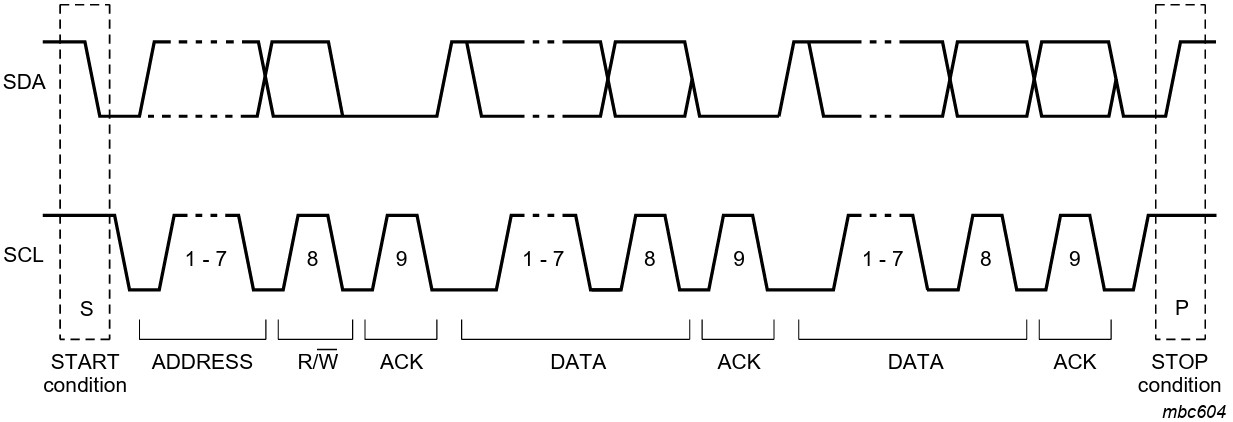
Figure 2 details the I2C frame structure, which is an 8-bit, MSB-first, bidirectional protocol. There are three components of communication for a simpler understanding.
- Transactions:
Transactions are framed by unique electrical conditions that occur only when the clock is HIGH.
- START Condition (S): Defined as a HIGH-to-LOW transition on SDA while SCL is HIGH. This alerts all devices on the bus to wake up and listen.
- STOP Condition (P): Defined as a LOW-to-HIGH transition on SDA while SCL is HIGH. This signals the end of the transaction and releases the bus to an idle state.
Note that during data transmission, SDA must remain stable while SCL is HIGH. It can only change state when SCL is LOW.
- Address handling:
The first byte following the START condition is the Address Frame. It contains:
- Target Address (7 bits): The unique identifier for the slave device.
- R/W Bit (1 bit): The LSB of this byte. A ‘0’ indicates a Write (Controller to Target), and a ‘1’ indicates a Read (Target to Controller).
- The 9th bit for the Acknowledge bit
Every byte transferred, whether address or data, is followed by a 9th clock pulse known as the Acknowledge (ACK/NACK) bit.
- ACK (Logic 0): The receiver pulls SDA LOW to acknowledge receipt of the byte.
- NACK (Logic 1): If the receiver leaves SDA HIGH, it is a Not-Acknowledge. This typically indicates a missing device, a busy device, or the end of a read sequence.
Case study
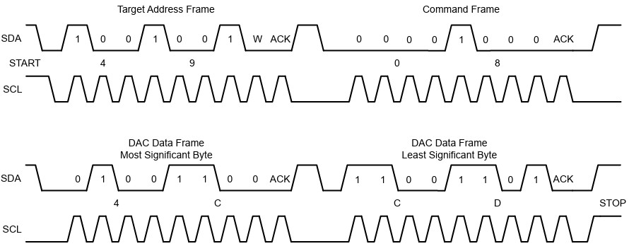
Here is a practical application of I2C communication at the hardware level to write a specific register inside a device. Figure 3 illustrates a multi-byte write to the DAC80501, a DAC from Texas Instruments.
The operation can be simplified into the following three components.
- Address Frame: Controller sends Address + Write bit (e.g., 0x49 + 0).
- Command Frame: Controller sends the register pointer (e.g., 0x08). This tells the DAC that subsequent data is destined for the DAC Data Register.
- Data Frames: Controller sends the 16-bit voltage value (MSB followed by LSB).
This establishes the standard workflow for actuators, which starts from Address, proceeds to Command, and then to Data.
Summary
Mastering I2C requires looking beyond the code libraries. It requires understanding that the HIGH state is passive, that the 9th bit (ACK) is the fundamental handshake of valid data, and that complex register access almost always involves a pointer-write followed by a Repeated Start.
References
Section 24. Inter-Integrated Circuit (I2C), Microchip Technology Inc.
I2C-bus specification and user manual, NXP Semiconductors
AN90044, A Study of I2C with Examples, Nexperia
Understanding the I2C Bus, Texas Instruments
A Basic Guide to I2C, Texas Instruments
EEWorld Online related content
How does a basic digital-to-analog converter (DAC) perform signal conversion?
The Internal Processor Bus: data, address, and control bus
What are built-in analog to digital converters?
Testing and debugging the I2C digital data bus
Looking for an alternative to I2C for sensors?
Basics of working with I2C buses
What is I2C


Leave a Reply