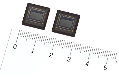
 Sony Semiconductor Solutions Corporation announced the upcoming release of two types of stacked event-based vision sensors. These sensors designed for industrial equipment are capable of detecting only subject changes and achieve the industry’s smallest* 1-pixel size of 4.86μm.
Event-based vision sensors asynchronously detect luminance changes for each pixel and output the changed data only, combining it with information on pixel position (xy coordinates) and time, thereby enabling high-speed, low latency data output.
The two new sensors employ stacking technology leveraging Sony’s proprietary Cu-Cu connection*2 to achieve the industry’s smallest* 1-pixel size of 4.86μm. In addition to operating with low power consumption and delivering high-speed, low-latency, high-temporal-resolution data output, the new sensors also feature a surprisingly high resolution for their small size. All of these advantages combine to ensure immediate detection of moving subjects in diverse environments and situations.
These two sensors were made possible through a collaboration between Sony and Prophesee, by combining Sony’s CMOS image sensor technology with Prophesee’s unique event-based vision sensing technology. This enables high-speed, high-precision data acquisition and contributes to improving the productivity of industrial equipment.
With the ever more sophisticated and diversified needs of the industrial equipment business,
the use of sensing to extract the necessary information from images captured by cameras continues to grow, demanding ever more efficient data acquisition.
With the frame-based method which is commonly used, the entire image is output at certain intervals determined by the frame rate. The new Sony’s sensors, however, utilize an event-based method that asynchronously detects pixel luminance changes and outputs data with pixel position (xy coordinates) and time information. They employ a proprietary stacked structure leveraging Cu-Cu connection to achieve conduction between the pixel chip and the logic chip, which is equipped with a signal processing circuit for detecting luminance changes, for each pixel. This design makes it possible that only the pixels that have detected a change in luminance for the object can output data, allowing the sensor to immediately detect the luminance changes with high-speed, low-latency, high-temporal-resolution while operating with low power consumption. Meanwhile, the design boasts the industry’s smallest 1-pixel size of 4.86μm, making for a very compact, high-resolution sensor.
These products can sense slight changes in vibration, detecting abnormalities for use in predictive maintenance of equipment. They also sense changes in sparks produced during welding and metal cutting, information which can be used to notify workers of the optimal time to change tools, among other possibilities. Likewise, they can contribute to improved production in various applications that frame-based image sensors have trouble with, as well as to support work processes that rely on the human experience.
The new sensors employ a proprietary stacked structure leveraging Cu-Cu connection to achieve conduction between the pixel chip and the logic chip, which is equipped with a signal processing circuit for detecting luminance changes, for each pixel. The pixel unit and signal processing circuit are typically placed on the same board. With these products, however, the unique structure delivers the industry’s smallest* 1-pixel size of 4.86μm while maintaining a high aperture ratio*4 for the pixel unit. This design delivers both a compact form factor and high resolution, providing high-precision recognition capabilities.
The proprietary stacked construction allowed Sony to opt for an event-based method that asynchronously detects pixel luminance changes and outputs data with pixel position (xy coordinates) and time information. Unlike the frame-based method, this allows the sensors to read only the required data, thereby saving on power consumption, but with microsecond-level high speed and low latency, enabling high-temporal-resolution output.
These sensors are equipped with event filtering functions developed by Prophesee for eliminating unnecessary event data, making them ready for various applications. Using these filters helps eliminate events that are unnecessary for the recognition task at hand, such as the LED flickering that can occur at certain frequencies (anti-flicker), as well as events that are highly unlikely to be the outline of a moving subject (event filter). The filters also make it possible to adjust the volume of data when necessary to ensure it falls below the event rate that can be processed in downstream systems (event rate control).
As part of the collaboration between Sony and Prophesee on these products, Metavision Intelligence Suite is available from Prophesee. Combining Sony’s event-based vision sensors with this software will enable efficient application development and provide solutions for various use cases.


Leave a Reply