
Generative artificial intelligence (AI) requires rapid and continuous movement of large amounts of data. In a growing number of instances, electrical input/output (I/O) connections between the ICs in chiplets are becoming a bottleneck to higher performance. Key electrical I/O performance barriers include power efficiency, bandwidth, and latency. This FAQ looks at the anticipated benefits of using in-package optical I/O (IOI) in place of today’s electrical I/O in chiplets and closes with a look at emerging IOI solutions and technologies.
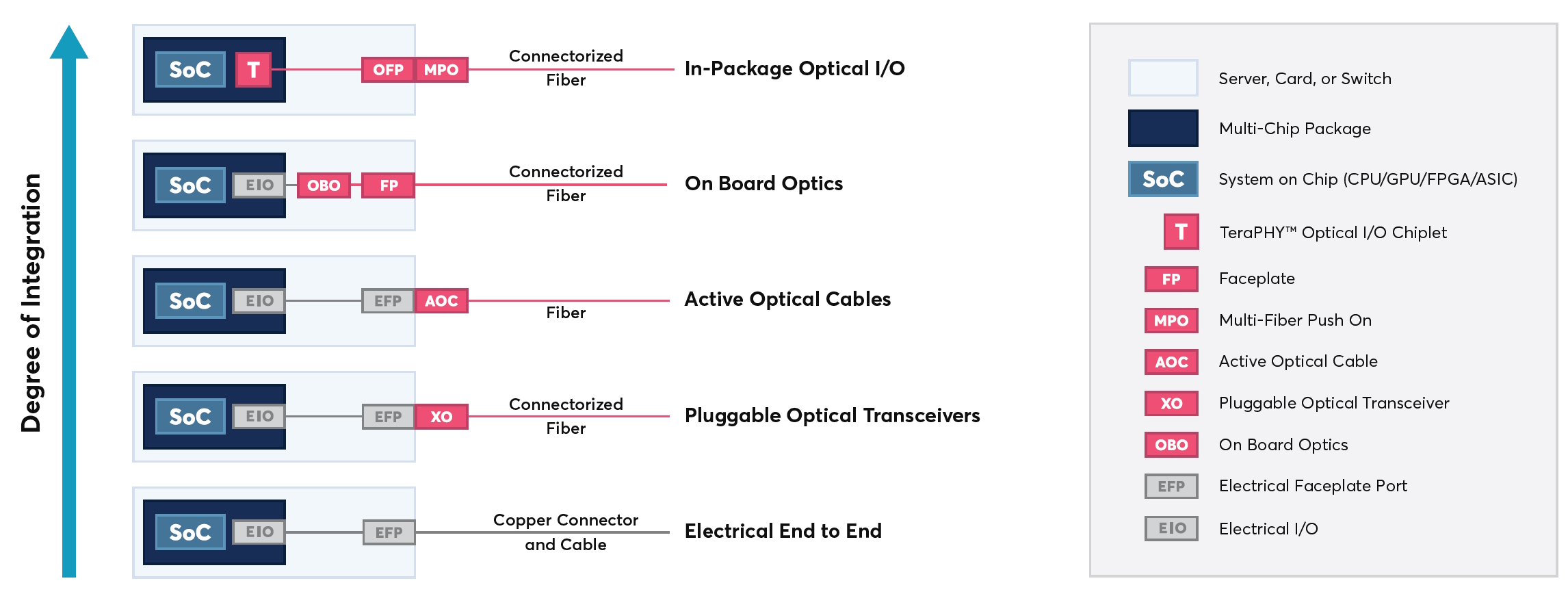
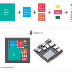
IOI solutions represent the latest in a long line of advancements in optical interconnects, beginning with pluggable optical transceivers replacing or supplementing electrical I/Os in data centers (Figure 1). For example, electrical Serializer/Deserializer (SerDes) is a common form of high-speed connectivity. It consists of a pair of blocks that convert data between serial data and parallel interfaces in each direction. However, exceeding 112 gigabits per second (Gbps) is extremely challenging because the large signal losses in copper interconnects make it hard to transmit data further than a few centimeters. The replacement of SerDes with OIO in chiplets is expected to eliminate electrical I/O bottlenecks and dramatically increase data transmission speeds. Critical barriers to increasing I/O performance include power efficiency, latency, and bandwidth density and reach.
I/O performance barriers
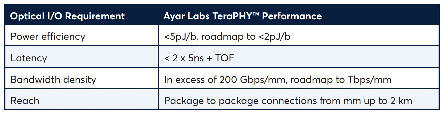
Power efficiency is critical for high-performance computing applications like generative AI. The power efficiency of existing electrical I/O at 112 Gbps is about 6 to 10 pico Joules per bit (pJ/b). Reaching from the package to the edge of a printed circuit board at that data rate is possible but takes a lot of power, generates heat, and reduces system efficiency. As noted in Figure 1, reaching beyond the edge of the PCB requires a mix of electrical I/O pluggable optical transceivers and active optical cables. IOI needs to improve on those performance levels.
Latency is another performance killer. On- and off-board electrical I/O at rates above 50 Gbps require the use of forward error correction coding that can increase latency by up to 100 ns. That’s too much for distributed computing systems like those used for generative AI. In those applications, latencies below 10 ns are required.
Bandwidth density is an important factor. Heterogeneous chiplets are used where high system density is demanded, and that includes bandwidth density. Electrical I/O can support a bandwidth density of about 100 Gbps/mm. The limit for SerDes is about 200 to 500 Gbps/mm; longer reach incurs power and thermal penalties, making it an impractical solution in most applications. IOI, on the other hand, can currently deliver about 200 Gbps/mm, with roadmaps expecting to achieve 1 Tbps/mm in the future.
Reach is the end-to-end distance of the I/O. In a chiplet, the needed reach is usually under 10 mm. On a PCB, the reach can be up to 50 mm, and in a data center, the reach can exceed 1,000 mm. While electrical I/O can support short reaches, longer distances require the use of optical communications. Switching between electrical communications inside the package or on the PCB to optical for longer reaches is inefficient and costly. A preferred solution would be to use IOI for both internal chiplet communications and data center-wide connectivity.
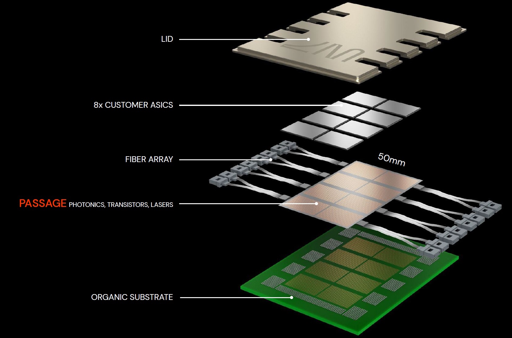
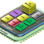
Several vendors have announced IOI solutions. In one case, a wafer-scale programmable photonic interconnect fabric has been developed for use in heterogeneous chiplets. The design supports 40 switchable photonic lanes in the same space occupied by a conventional optical fiber. Initial implementations are expected to support speeds of 1 Tbps across arrays on up to 48 heterogeneous ICs on substrates up to 8 inches square with a maximum latency of 5 ns and lower power consumption compared to alternative electrical I/O (Figure 2). The architecture is expected to scale to bandwidths up to 100 Tbps.
A second approach uses a multiwavelength optical source that combines silicon photonics with standard CMOS processing to deliver up to 1000x higher bandwidth density at 10% of the power consumption of electrical I/O (Table 1). The solution uses a high-volume GlobalFoundries 45-nanometer process to integrate millions of transistors with hundreds of photonic devices.
Summary
The I/O requirements of advanced generative AI and other high-performance computing (HPC) applications exceed the capabilities of electrical-based solutions. As a result, IOI technologies are being developed that can support the power efficiency, latency, bandwidth efficiency and reach demands of HPC applications.
References
Heterogeneous Integration Roadmap, 2023 edition, Chapter 9: Integrated Photonics, IEEE
Lightmatter Passage brings Co-Packaged Optics and Silicon Photonics to the Chiplet Era, ServeTheHome
Optical Interconnect for Hyperscale Data Center with AI / ML Applications, Amphenol
Optical Interconnects Finally Seeing the Light in Silicon Photonics: Past the Hype, MDPI nanomaterials
Photonics Keynote: Transitioning from Electrical to Optical I/O, Cadence
Polycrystalline silicon PhC cavities for CMOS on‑chip integration, Scientific Reports
Rethinking Generative AI Architectures with Optical I/O, Ayer Labs

Leave a Reply