Chiplet testing begins with performance simulations during the design process. Compared with monolithic devices, heterogeneous chiplets require more complex testing, including known good die (KGD) testing, final test, and system level test. Success also depends on the implementation of design for test (DfT) based on several IEEE standards.
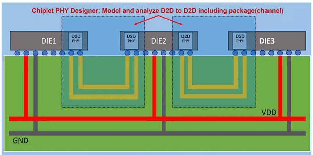
Chiplet designers need high-speed tools that can quickly and precisely simulate the die-to-die (D2D) interconnects, which are one of the keys to chiplet performance. For an increasing number of chiplets, simulation, and verification that the design meets the specifications of the Universal Chiplet Interconnect Express (UCIe) standard is another key consideration.
UCIe is important for interconnects between chiplets and within chiplets. Simulation of chiplet physical (PHY) layer includes several factors:
- Support for the UCIe PHY standard, including automated parsing of signals and automated connections between multiple dies.
- Precise computation and verification that the voltage transfer function (VTF) complies with UCIe specifications. That includes analysis of system bit error rates (BERs) and quantification of eye diagram parameters, including height, width, skew, and mask margins.
- Accurate analysis of forward clocking to capture asynchronous behavior.
These tests are required to validate the performance of chiplet subsystems from one D2D PHY through the substrate interconnects and to a second D2D PHY (Figure 1).
Once the design is complete, fabrication of chiplets begins with testing the individual chips to identify KGD before assembly can begin. All aspects of chip performance must be verified, otherwise problems can crop up later in final testing and system testing. In addition to using KGD, it’s necessary to perform detailed system-level testing. Chiplets include a heterogeneous mix of process nodes and materials. Those various dies can have different temperature characteristics, different reactions to electromagnetic interference (EMI), and other performance challenges like electromigration.
Especially with complex systems like chiplets, DfT is an important consideration. DfT technologies have been developed over an extended time for systems ranging from printed circuit boards to systems on chip (SoC) and, more recently, for chiplets. DfT capabilities need to be built into the dies used for chiplets.
IEEE 1838 DfT for chiplets
To address the needs of testing 2.5D and 3D devices like chiplets, the IEEE has developed and updated several standards, including (Table 1):
- IEEE 1149.1 (JTAG), Standard for Test Access Port and Boundary-Scan Architecture test access standard for packaged ICs on a printed circuit board
- IEEE 1149.6, Standard for Boundary-Scan Testing of Advanced Digital Networks, is used for testing high-speed differential and AC-coupled interconnects between chips on PCBs and systems.
- IEEE 1500, Standard Testability Method for Embedded Core-based Integrated Circuits. Test access standard for embedded cores in a large system-on-chip (SoC).
- IEEE 1687, Standard for Access and Control of Instrumentation Embedded within a Semiconductor Device.
- IEEE P1838, Standard for Test Access Architecture for Three-Dimensional Stacked Integrated Circuits.
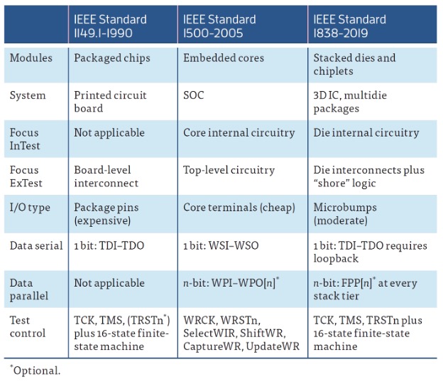
IEEE 1838 applies to dies that are intended to be part of a multi-die stack. It includes specifications for 3D interoperability between multiple die chiplets and interfacing with other standards. It defines die-level features needed to enable a series of compliant dies to operate in a stack-level architecture that enables the transport of the control and data signals required for testing, including intra-die interconnects and inter-die interconnects.
Although IEEE 1149.1 and 1149.6 were developed for PCB-based systems, multi-die devices like chiplets and D2D interconnections can be tested using the same or very similar methodologies. IEEE 1149.1 and 1149.6 can be used in serially accessible IEEE 1687 or IEEE 1500 scan networks. For example, boundary scanning is a static vector-based technique that uses on-chip embedded circuitry to implement structural testing. It can identify shorts, open stuck-at, and bridging faults. It can be used to identify faults in single-ended and differential nets.
Summary
Chiplets are complex assemblies, and chiplet testing is a complex process. It begins with simulation, extends to KGD testing before assembly, and includes det assemblies. There are several IEEE standards that provide guidance for chiplet testing.
References
Chiplet Interconnect Testing Using JTAG/Boundary Scan, Asset Intertech
Ensuring the Health and Reliability of Multi-Die Systems, Synopsys
IEEE Standard 1838 Is on the Move, IEEE Computer Society
Keysight Introduces Chiplet PHY Designer for Simulating D2D to D2D PHY IP Supporting the UCIe™ Standard
Synopsys and Intel Team Up on the First UCIe-Connected Chiplet-Based Test Chip, Synopsys
Tackling Complex Challenges in Semiconductor Chiplet Testing, Elevate Semiconductor
Test Strategies in the Era of Heterogeneous Integration, Teradyne
Leave a Reply