Solid-state memory devices are available in a wide variety of standard package styles that they have in common with other semiconductor devices, including DIP, TSSOP, DFN, WLCSP, and many others. And various packages are offered in plastic, glass, ceramic, and metal containing one or more devices. They are also available in hermetically-sealed packages and non-hermetic packages. In the case of memory devices, however, several types of application-specific package configurations have been developed, as described below.
DIMM, SO-DIMM, MicroDIMM, and NVDIMMs
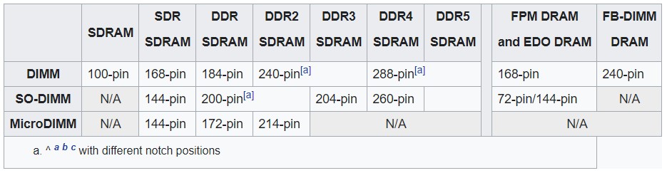
Memory is available in a variety of module forms with from 72 pins to 200 pins. Common forms include dual inline memory modules (DIMMs), small outline dual inline memory modules (SO-DIMMS) and MicroDIMMs. SO-DIMMs are about half the size of the corresponding DIMMs and are designed for use in portable devices such as notebook computers. A MicroDIMM module has a smaller outline and thickness than standard SO-DIMM modules. MicroDIMMs are designed for mobile devices and slim and super lightweight notebooks.
Some forms of persistent memory are offered in a module package based on NVDIMMs. Micron offers NVDIMMs that operate in the DRAM memory slots of servers to handle critical data at DRAM speeds. In the event of a power failure or system crash, an onboard controller transfers data stored in DRAM to the onboard nonvolatile memory, thereby preserving data that would otherwise be lost. When the system stability is restored, the controller transfers the data from the NAND back to the DRAM, allowing the application to pick up where it left off efficiently.
3D memory
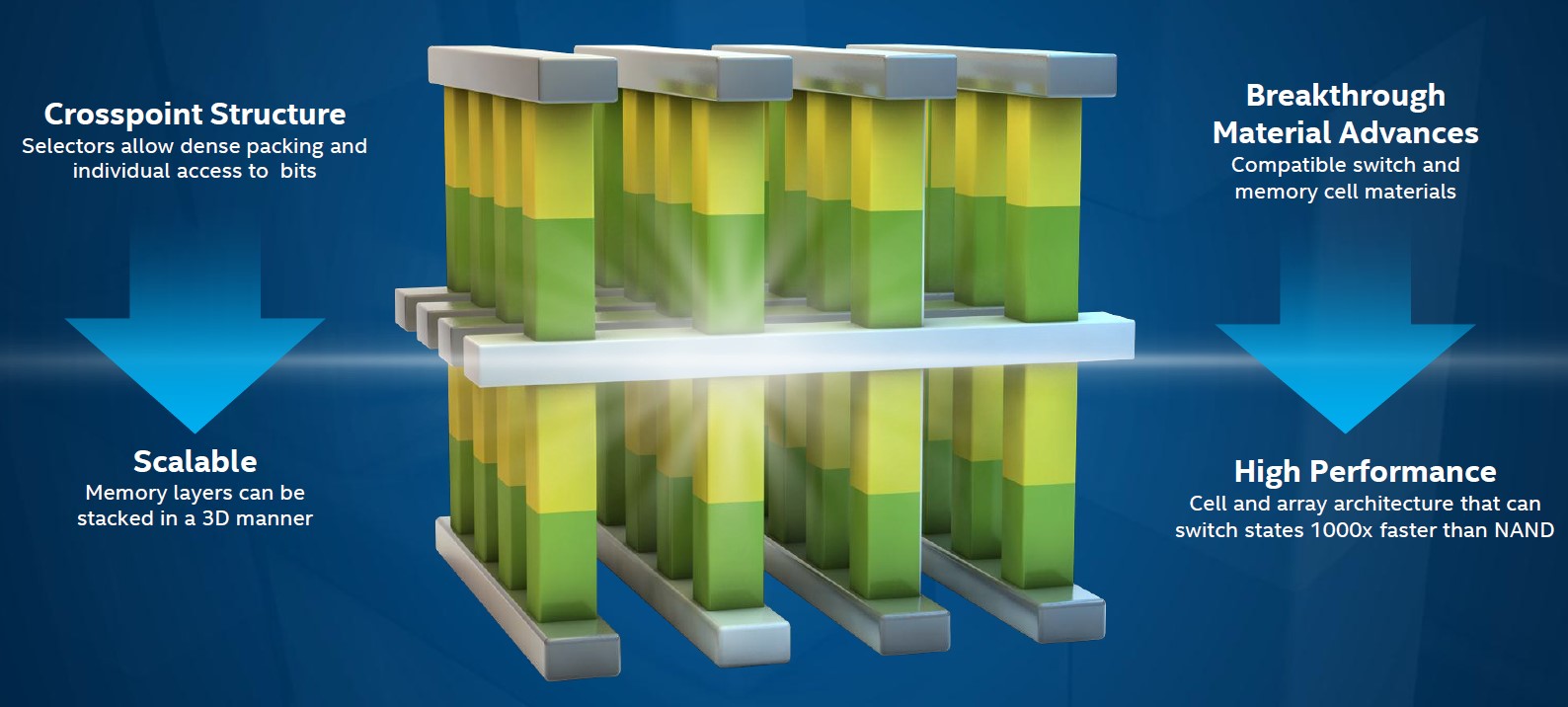
Intel and Micron have co-developed a 3D memory technology used to supply persistent memory. Called Optane by Intel and 3D XPoint™ by Micron, this technology stacks memory grids in a three-dimensional matrix. This architecture improves density, increases performance, and provides persistence. It enables like DRAM (byte addressability, high endurance, write in place) or traditional storage (block addressability, persistence), depending on the use case of product configuration.
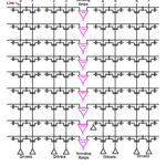
High Bandwidth Memory (HBM) is a 3-dimensional SDRAM structure developed for use with high-performance graphics accelerators, network devices, and high-performance computing. It is an interface structure for 3D-stacked SDRAM from Samsung, AMD, and SK Hynix. JEDEC adopted HBM as an industry-standard in October 2013. The second generation, HBM2, was accepted by JEDEC in January 2016.
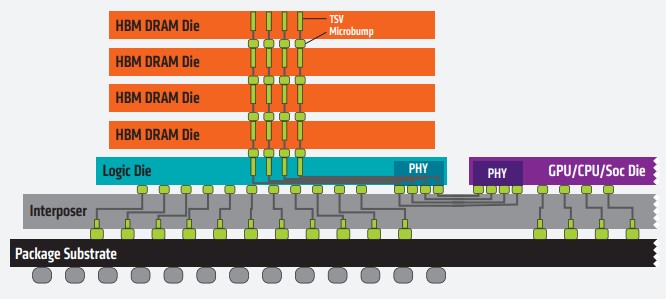
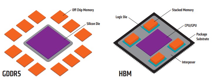
According to AMD, although these HBM stacks are not physically integrated with the CPU or GPU, they are so closely and quickly connected via the interposer that HBM’s characteristics are nearly indistinguishable from on-chip integrated RAM. And HBM resets the clock on memory power efficiency, offering >3X the bandwidth per watt of GDDR5. Beyond performance and power efficiency, HBM also saves system space. Compared to GDDR5, HBM can fit the same amount of memory in 94% less space.
Package on package
A predecessor to 3D memory structures, package on package (PoP) technology is a technique that vertically combines discrete logic and memory ball grid array (BGA) packages. While today’s 3D memory technologies are aimed at high-performance systems, PoP was developed initially for use in mobile and small-format devices. As a result of thermal management challenges with PoP, stacks of more than two devices are not common. The stack can consist of several memory devices, or a combination of memory and a processor.
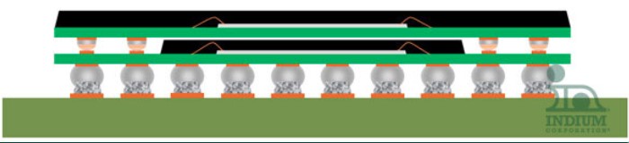
PoP assembly is most commonly carried out using a no-clean process by printing solder paste onto the substrate and placing the logic chip into the paste. The memory package is then either dipped into a specially-designed PoP flux or solder paste and placed on top of the logic chip. The whole assembly is then reflowed.
Embedded memory
Integrated on-chip memory is referred to as embedded memory. It can be used for cache memory and other functions and can be comprised of various memory technologies, including RAM, ROM, flash, EEPROM, and so on. It directly supports the operation of the logic functions on the chip. High-performance embedded memory is a critical element in VLSI devices, including standard processors and custom ICs. Embedding memory on the ASIC or processor allows for much wider buses and higher operation speeds. In the case of power-conscious applications such as wearables or wireless IoT sensors, embedded memory can be used to dynamically reduce power consumption by controlling data transfer speeds based on real-time conditions.
The third and final FAQ in this series considers “Memory Centric Computing and Memory System Architectures.”
References
3D XPoint Introduction, Micron
DIMM, Wikipedia
High Bandwidth Memory, AMD
Intel Optane Technology, Intel
NVDIMM, Micron
Package-on-Package Fluxs, Indium Corp.


Leave a Reply