RDS(on) stands for “drain-source on resistance,” or the total resistance between the drain and source in a Metal Oxide Field Effect Transistor, or MOSFET when the MOSFET is “on.” RDS(on) is the basis for a maximum current rating of the MOSFET and is also associated with current loss. All things being equal, the lower the RDS(on), the better.
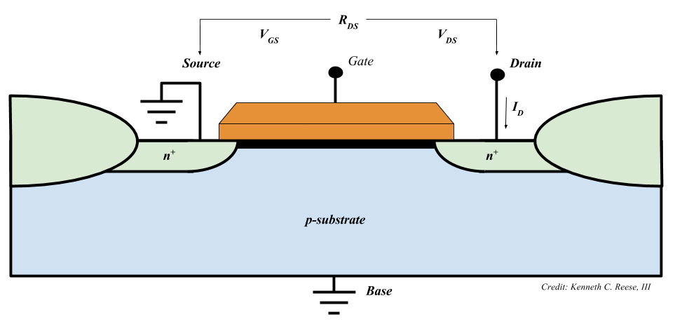
MOSFETs make perfect switching devices and are often used in power applications. Example applications for power MOSFETs include Switched Mode Power Supplies (SMPS), motor control, automotive, and in any application where a heavy-duty electronic switch is needed, such as a driver. Current flows between the n-channels when a gate-to-source voltage (VGS) is applied, otherwise the MOSFET behaves like a resistor. When VGS reaches the threshold voltage VGS(th), an inversion layer forms that enables current flow. The inversion layer becomes the conductive path (or channel) of the MOSFET between drain and source.
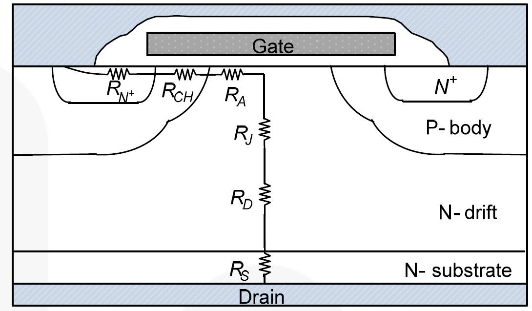
RDS(on), the total resistance in the path from source to drain, is made up of a series of resistances that traverses the path of current flow. RN is the source region’s diffusion resistance. RCH is the channel region’s resistance. RA is the resistance of an area called the accumulation region. RJ is the resistance of an area called the JFET region. RD is the drift region resistance and the most important factor in high-voltage MOSFETs. RS is the resistance of the substrate itself and can be ignored in high-voltage MOSFETs. However, in low voltage MOSFETs it can have a large effect on RDS(on). See Figure 2 of a vertical structure of a MOSFET and a series of resistances in series forms the total RDS(on) in the path of current flow from source to drain.
Besides these inherent structural contributors to RDS(on), imperfect contact between the source and drain metal and even the wiring that connects the die to the leads on the package can also contribute to RDS(on).[i] The latter can be identified as RWCML, or the total of the bond wire resistance, contact resistance, and the resistance of the lead frame.[ii]
RDS(on) increases with increasing temperature (this is also known as a positive temperature coefficient.) This is because of the mobility of the hole and electron decrease with increasing temperature.
RDS(on) is a function of temperature as defined by the following formula:
RDS(on) (T) = RDS(on) x (25°C) x (T/300)2.3, where T is absolute temperature.[i]
[i] AN-9010 MOSFET Basics. (2000). ON Semi Application Note, 1-17. Retrieved April 30, 2017.
[ii] IDAN0061 Power MOSFET Basics. Abdus Sattar, IXYS Corp. Retrieved April 30, 2017.
Im curious. RDS on was once measured in ohms to calculate the power consumed by the device. New RDS on in megohm figures seem confusing.
Can you bridge the information gap for me on this point?
Megohm, u mean miliohm? most modern mosfet datasheets measure RDS(on) in miliohms, as in 1 thousandth of an ohm, it just means that modern transistors are more efficient
This confused me too! But, milliOhm makes way more sense. The difference between M and m is huge!