Rambus Inc. announced it has expanded its portfolio of high-speed interface IP on TSMC’s industry-leading 7nm process with the addition of its silicon-demonstrated 112G XSR/USR PHY. Offering unmatched power and area efficiency for next-generation applications, the 112G XSR/USR PHY is a critical enabler of chiplet and CPO architectures for data center, networking, 5G, HPC and AI/ML applications.
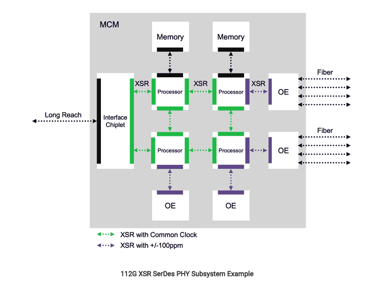
 The accelerated trend of disaggregation of large SoCs into multiple smaller chiplets demands faster time to market, yield improvement and design flexibility. The Rambus 112G XSR/USR PHY is a critical enabler of the D2D and D2OE interconnects for chiplet architectures. Implemented on TSMC’s advanced process technology, this chiplet connectivity solution has been demonstrated in silicon to exceed the challenging reach/BER performance of the CEI-112G XSR specification, and supports NRZ and PAM-4 signaling at various data rates for maximum design flexibility.
Leading-edge applications moving to chiplet architectures include next-generation 51.2 Terabit per second (Tbps) ASICs for network switches, where 112G XSR links will connect the digital switch ASIC die to CPO engines. In AI/ML and HPC SoCs, the 112G XSR PHY can be used to bridge purpose-built accelerator chiplets for natural language processing, video transcoding and image recognition. Another popular use case is the die disaggregation of large SoCs, hitting reticle size limits for manufacturable yields, into multiple smaller die connected using XSR links over organic substrate. Increasingly, these advanced applications are implemented on TSMC’s N7 process.
Leave a Reply