• Skip to primary navigation
  • Skip to main content
  • Skip to primary sidebar
  • Skip to footer

Microcontroller Tips

Microcontroller engineering resources, new microcontroller products and electronics engineering news

  • Products
    • 8-bit
    • 16-bit
    • 32-bit
    • 64-bit
  • Applications
    • 5G
    • Automotive
    • Connectivity
    • Consumer Electronics
    • EV Engineering
    • Industrial
    • IoT
    • Medical
    • Security
    • Telecommunications
    • Wearables
    • Wireless
  • Learn
    • eBooks / Tech Tips
    • EE Training Days
    • FAQs
    • Learning Center
    • Tech Toolboxes
    • Webinars/Digital Events
  • Resources
    • Design Guide Library
    • LEAP Awards
    • Podcasts
    • White Papers
  • Videos
    • EE Videos & Interviews
    • Teardown Videos
  • EE Forums
    • EDABoard.com
    • Electro-Tech-Online.com
  • Engineering Training Days
  • Advertise
  • Subscribe

3D image sensor billed as world’s smallest

January 9, 2020 By Aimee Kalnoskas Leave a Comment

REAL3 3D image sensor
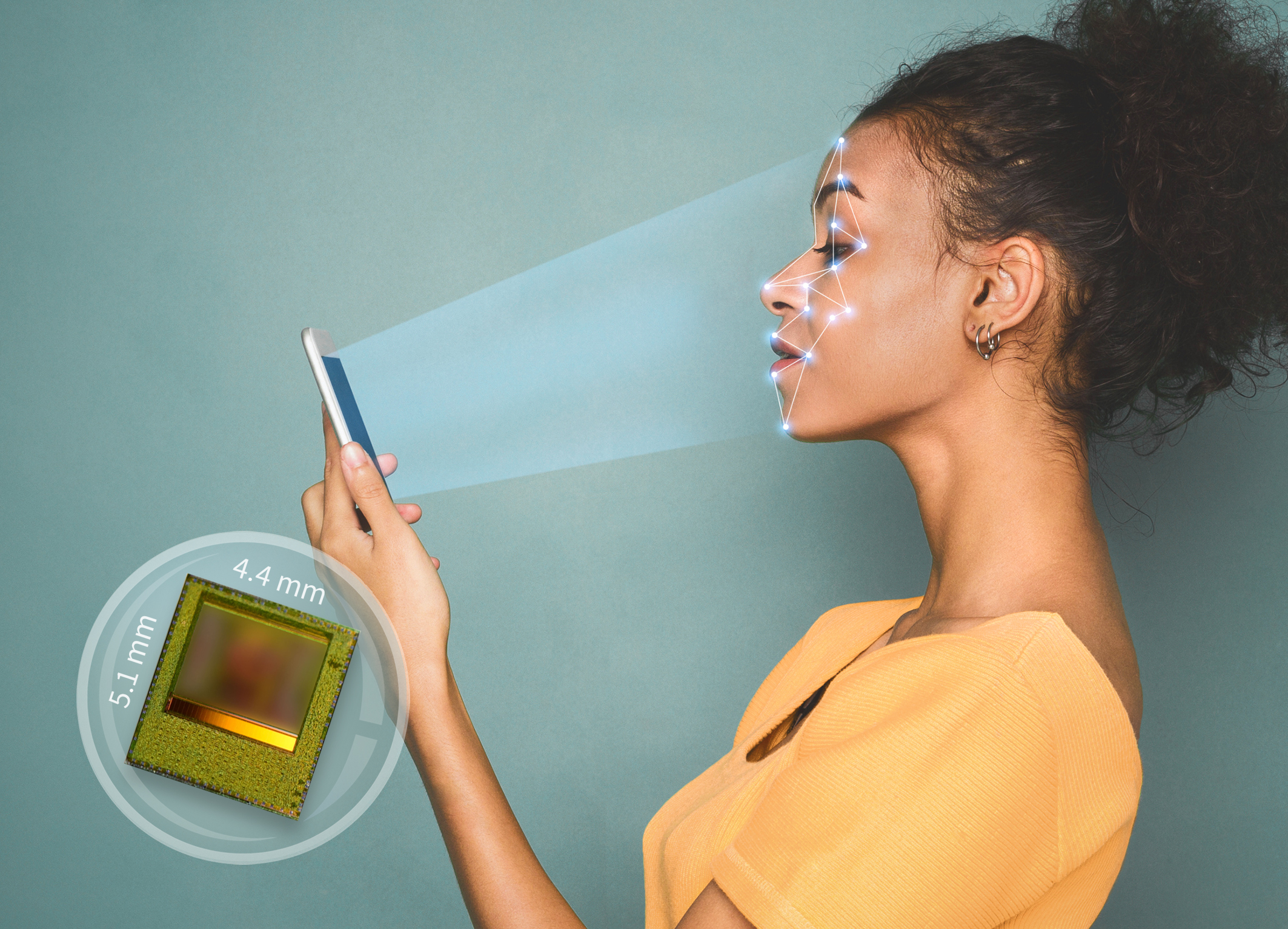
Reliable face authentication, improved photo functions, and authentic augmented reality experiences: 3D depth sensors assume a key role in smartphones and for applications that rely on accurate 3D image data. Infineon Technologies AG has collaborated with software and 3D Time of Flight system specialist pmdtechnologies ag to develop the world’s smallest and most powerful 3D image sensor.

The new REAL3 single-chip solution measuring just 4.4 x 5.1 mm, is the fifth generation of successful time-of-flight deep sensors from Infineon. Its small dimensions allow it to be incorporated into the smallest devices with just a few elements. The chip also provides the highest resolution data with low power consumption.

The new REAL3 chip meets a range of applications in the areas of security, image use and context-based interaction with the devices. The 3D sensor also allows the device to be controlled via gestures, so that human-machine interaction is context-based and without touch.

The depth sensor time-of-flight technology enables an accurate 3D image of faces, hand details or objects which is relevant when it must be ensured that the image matches the original. When applied in payment transactions using mobile phones or devices that need no bank details, bank cards or cashiers, the payment is carried out via facial recognition. This requires an extremely reliable and secure image and return transmission of the high-resolution 3D image data. The same applies to securely unlocking devices with a 3D image. The Infineon 3D image sensor also implements this in particular in extreme lighting conditions such as strong sunlight or in the dark.

Furthermore, the chip provides additional options for ambitious photos with cameras, for example, with enhanced autofocus, bokeh effect for photo and video, and improved resolution in poor lighting conditions. Real-time full-3D mapping also allows authentic augmented reality experiences to be presented.

Series production will begin in the middle of 2020. In addition, Infineon Technologies offers an optimized illumination driver (IRS9100C) that further improves performance, size and cost as a complete solution. More information on Infineon’s 3D image sensor family can be found at www.infineon.com/real3.

You may also like:

  • LIDAR and Time of Flight
    LiDAR and Time of Flight, Part 4: Circuitry and advances
  • LIDAR and Time of Flight
    LiDAR and Time of Flight, Part 3: Emitters, sensors, and…

  • LiDAR and Time of Flight, Part 2: Operation
  • LIDAR and Time of Flight
    LiDAR and Time of Flight, Part 1: Introduction
  • Inertial Measurement Units
    Inertial Measurement Units: The hidden key to Apollo success, now…

Filed Under: microcontroller, Sensor modules Tagged With: infineontechnologiesag

Reader Interactions

Leave a Reply Cancel reply

Your email address will not be published. Required fields are marked *

Primary Sidebar

Featured Contributions

Navigating the EU Cyber Resilience Act: a manufacturer’s perspective

The intelligent Edge: powering next-gen Edge AI applications

Engineering harmony: solving the multiprotocol puzzle in IoT device design

What’s slowing down Edge AI? It’s not compute, it’s data movement

Five challenges for developing next-generation ADAS and autonomous vehicles

More Featured Contributions

EE TECH TOOLBOX

“ee
Tech Toolbox: Power Efficiency
Discover proven strategies for power conversion, wide bandgap devices, and motor control — balancing performance, cost, and sustainability across industrial, automotive, and IoT systems.

EE Learning Center

EE Learning Center

EE ENGINEERING TRAINING DAYS

engineering
“bills
“microcontroller
EXPAND YOUR KNOWLEDGE AND STAY CONNECTED
Get the latest info on technologies, tools and strategies for EE professionals.

Footer

Microcontroller Tips

EE World Online Network

  • 5G Technology World
  • EE World Online
  • Engineers Garage
  • Analog IC Tips
  • Battery Power Tips
  • Connector Tips
  • EDA Board Forums
  • Electro Tech Online Forums
  • EV Engineering
  • Power Electronic Tips
  • Sensor Tips
  • Test and Measurement Tips

Microcontroller Tips

  • Subscribe to our newsletter
  • Advertise with us
  • Contact us
  • About us

Copyright © 2025 · WTWH Media LLC and its licensors. All rights reserved.
The material on this site may not be reproduced, distributed, transmitted, cached or otherwise used, except with the prior written permission of WTWH Media.

Privacy Policy