Tricks of the trade for optimizing the energy consumption of BLE chips affect memory size, clock speed, operating modes, and other factors determined during the initial design.
Emmanuel Sambuis, Silicon Labs
It can be challenging to optimize Bluetooth Low Energy (BLE) applications for minimal energy consumption. An understanding of BLE and the underlying system-on-chip (SoC) architecture is critical for realizing extended battery life. Particularly important are insights into the BLE modes of operation (such as Advertising and Sleep). There are different ways to minimize the power consumption of the entire system by providing the right inputs to the stack and taking advantage of hardware features of BLE SoCs.
Within Bluetooth, BLE has secured a significant number of sockets. One of the most critical reasons for selecting BLE in a wireless design is its ubiquity thanks to its large deployment in smartphones and its ability to extend the battery life-time. Long battery life is extremely valuable as most IoT end nodes are battery operated.
Though it may sound obvious, the selection of a BLE device starts with the evaluation of its documentation. While the initial data-mining process seems trivial, the comparison of semiconductor device data-sheets can quickly turn into a complicated task.
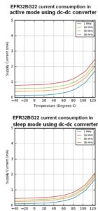
Consider, for example, the active current in the wireless SoC’s receive or transmit modes. Many BLE SoCs report a current consumption of a few milliamps. For instance, the EFR32BG22 SoC from Silicon Labs has a radio-receive current of 2.6 mA and a transmit current of 3.5 mA at 0 dBm. Note these numbers only relate to the SoC RF transceiver. At the SoC level, these currents are slightly higher, 3.6 mA and 4.1 mA respectively. Relying only on the radio numbers for the SoC current drain is a common mistake. The front-page of the device documentation often must be validated with a thorough analysis of the data-sheet.
Another example is the CPU power consumption reported in microamps-per-megahertz. This number can become a decisive selection criterion in the case of intensive compute applications. It is typically reported in the best-case scenario, which is often the maximum frequency of the CPU. In other words, the value shown in the data-sheet could prove to be vastly inaccurate when the SoC CPU works at a different frequency than that specified in the manufacturer’s documentation.
A third example is the deep-sleep current, critical for battery-operated end products. This number typically ranges between hundreds of nanoamps to a few microamps. It is essential to ensure the deep-sleep current numbers are associated with the size of the RAM retained and include the real-time-clock (RTC) current consumption. The RTC, combined with an accurate sleep clock source, is used to maintain the timing necessary for proper BLE operation. In the case of the EFR32BG22 SoC, the front page of the data-sheet mentions a deep-sleep current of 1.40 µA in EM2 mode with 32 kB of RAM retained and the RTC running from the LXCO (low-frequency crystal oscillator). The current consumption section of the data-sheet provides additional information.
Thus the lack of standardization for power numbers in datasheets can produce erroneous comparisons that could ultimately lead to selecting the wrong device.
Understanding application requirements
It is important to consider the application requirements when assessing BLE SoCs. Most suppliers try to represent their numbers responsibly, but it is impossible to treat all use cases for a device that might serve in dozens of different applications. This is where knowledge of the end application becomes critical.
Active and sleep currents are key specifications when selecting a BLE SoC. These current numbers must be inserted into a model that closely matches the application environment to produce a fair estimate of the average power consumption. Such models typically include the ON/OFF duty-cycle, knowing that a low duty cycle will favor an SoC with the lowest deep-sleep current. A high duty cycle will favor an SoC with the lowest active current.
Another parameter could be the ambient temperature of the end product, understanding that the leakage current of a BLE SoC at 25°C is significantly different from the leakage at 85°C or higher. The leakage current at a high temperature can be a key selection criterion in industrial applications such as sub-metering, which need a guaranteed battery life at high temperatures.
An additional important element of the application relates to the type of battery technology used (in the context of battery-operated end products). The battery powers the on-chip dc-dc converter integrated in the latest BLE SoCs. Using the dc-dc converter will significantly reduce the active current consumption of the entire SoC. Some sophisticated SoCs may integrate separate dc-dc converters for the radio and for the CPU. This practice provides an optimized solution, but the trend is clearly to have only one converter to minimize the cost of the SoC.
Finally, it is also important to understand how on-chip or off-chip memories are used. A common requirement for BLE end nodes is to perform over-the-air (OTA) updates of software. Depending on the size of the image to be transferred, an external flash device can be economical. But its added power consumption and potential for security problems can, however, prove to be quite higher than that when using on-chip flash. A detailed analysis of the OTA updates will help determine the most appropriate memory bill-of-material.
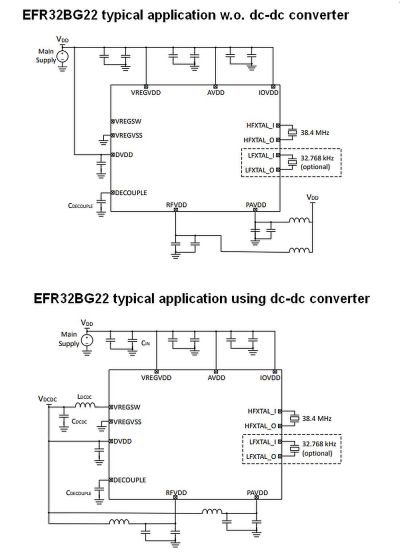
In recent years, BLE SoCs have significantly reduced their total active current consumption while maintaining a low deep-sleep current. The reason is the migration of silicon technology from larger geometries (0.18 µm, 90 nm and 65 nm) to much more optimized technology nodes (55 nm and 40 nm). Use of 40-nm geometry combined with the integration of an on-chip dc-dc converter has tremendously reduced the overall current consumption of the EFR32BG22 SoC.
For example, the Arm Cortex-M33 CPU requires 54 µA/MHz when running Coremark from the on-chip flash when the on-chip dc-dc converter is disabled. The same operation only requires 37 µA/MHz when the same dc-dc converter is activated.
In deep-sleep mode, the RAM retention is critical, both because it can represent a significant portion of the power budget and because RAM retention will allow a faster boot when the BLE SoC must return to active mode. From a design perspective, the use of low-leakage SRAM blocks has enabled silicon designers to keep the deep-sleep current in the range of 1µA. An additional key consideration when selecting a BLE SoC is the size of each SRAM block that can vary. The ability to select the size of the RAM to be retained will help minimize power consumption in deep-sleep mode. The EFR32BG22 SoC integrates independently selectable SRAM blocks for a total of 32 kB of on-chip RAM.
Finally, the combination of clock gating and power gating techniques allow the BLE SoC to completely shut down certain portions of the device depending on its mode of operation. The activation of these features is automatic, and their details are almost invisible to application developers.
Software enablement
Minimizing power consumption in BLE applications requires highly optimized scheduling of radio activity, maximizing the time spent in the lowest possible energy mode while maintaining the precise timing the protocol requires. To accurately control transmitted power, the BLE stack integrates the configuration of the dc-dc converter. The stack comes via a software development kit (SDK), which is fully integrated with an integrated development environment (IDE). The IDE includes a network analyzer that captures data directly from the SoC radio. An advanced energy monitor also correlates power consumption to code location. A visual GATT configurator is included to enable implementation of standard Bluetooth SIG profiles or custom services. These tools allow development of BLE applications that are fully integrated with the hardware design, allowing developers to focus on higher level design choices that affect power consumption. Also integrated into the SDK is secure bootloader support for firmware updates, both OTA and through a serial interface.
The combination of sophisticated hardware and powerful software enables application developers to perform their own benchmarking on multiple devices. This is the recommended approach that should be taken before selecting a BLE SoC. While initially more time consuming, this approach proves to be extremely valuable and helps reveal hidden challenges resulting from either missing hardware features or non-optimal software capabilities.
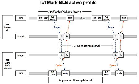
The development of a standardized benchmarking strategy can also help developers compare devices from multiple suppliers. The IoTMark-BLE benchmark profile developed by the Embedded Microprocessor Benchmark Consortium (EEMBC) provides a useful tool for assessing power consumption. The IoTMark-BLE benchmark profile models a real-world IoT edge node consisting of an I2C sensor and a BLE radio through sleep, advertise and connected-mode operations.
While this IoTMark-BLE benchmark might not suit all use cases, it can serve as a foundation for developing appropriate scenarios for any given application.
In a nutshell, side-by-side comparisons of vendor datasheets can lead to costly misunderstandings and misrepresentations. The analysis of BLE SoCs must take place at a system level as illustrated when comparing on-board and external dc-dc converter blocks within an SoC. Third-party benchmarks can often help determine what the comparative analysis should look like.
Mark Orchard-Webb, Silicon Labs, contributed the software enablement paragraph in this article.


Leave a Reply