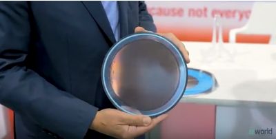
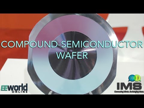
David Danzilio from Wind Semiconductor sat down with us to explain some of the basics behind fabricating wafers in the compound semiconductor area. Compound semiconductors have a lot of commercial applications in optoelectronics. Many have a direct bandgap that makes them efficient light emitters. (As a quick review, the band gap is called direct if the crystal momentum of electrons and holes is the same in both the conduction band and the valence band — an electron can directly emit a photon. In an indirect gap that characterizes silicon and germanium, a photon cannot be emitted because the electron must pass through an intermediate state and transfer momentum to the crystal lattice.)
 Wind is said to be the world’s largest compound semiconductor foundry. Its products go into the wireless communications industry as well as the optical networks and defense industries. Chips fabbed on Wind wafers find their way into most consumer products and into the wireless networks that transport data and deliver it to the mobile user.
First the basics: A compound semiconductor is a single-crystal semiconductor material composed of two or more different elements. Some of the widely used compound semiconductors include GaN, AlN, InSb, and GaAs from the III–V element groups and CdS, ZnSe, and HgTe from the II–VI groups.
The most widely used way of creating circuits on compound semiconductor wafers is through metalorganic vapor phase epitaxy (MOVPE). It uses ultrapure metalorganics and/or hydrides as precursor source materials in an ambient gas such as hydrogen. But there are other fabrication techniques used as well. They include molecular beam epitaxy (MBE), hydride vapor phase epitaxy (HVPE), liquid phase epitaxy (LPE), metal-organic molecular beam epitaxy (MOMBE), and atomic layer deposition (ALD).
Compared with silicon semiconductors, compound semiconductors are far more expensive and much more difficult to produce. Compound semiconductor substrates that include silicon carbide (SiC), gallium arsenic(GaAs), gallium phosphorus(GaP) and gallium nitride are being used for LEDs. III-V compound semiconductor devices have an ability to function at higher frequencies, and the exploding demand in commercial broadband/wireless communication and optical communication technologies has led to wide application of compound semiconductor process technology in high frequency, high power, low noise, and optoelectronic products.
Danzilio says WIN’s technology team has substantial experience in GaAs heterojunction bipolar transistor (HBT) and high-electron-mobility-transistor (HEMT) monolithic microwave integrated circuit (MMIC) fabrication. He says the team is familiar with the latest developments in GaAs technology and will provide continuous research and development to meet technology requirements.
In addition to MMIC technology, WIN has also established optoelectronic device technology such as compound semiconductor lasers and photodiodes. The service embodies Epi-wafer growth, optoelectronic device fabrication, and device characterization.
Win also fabricates multi-project masks where multiple customers will submit their designs and essentially buy a quarter wafer, as a means of lowering engineering cost.


Leave a Reply