
We take a look at the venerable Sony game box with an eye toward power handling and architecture.
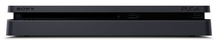
Chances are that if you’re a gamer, you’re experiencing your video games on a Sony PlayStation 4. To date, over 75 million PlayStation 4 boxes have sold. The closest competitor is the Xbox One (36.03 million) and the Switch (14.46 million). The PlayStation 4 now accounts for 60% of the gaming market, the Xbox One just 29%, and the Switch a mere 11%.
 With those statistics in mind, it’s understandable that the PlayStation 4 has gotten a lot of scrutiny. It’s possible to find a number of PlayStation 4 teardowns with an emphasis on taking the box apart for either repair or refurbishment purposes. Here, we’re more interested in the design decisions that went into devising the game box.
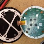
The PlayStation 4 does disassemble relatively easily if you have the right torx screwdrivers. The only complication we encountered were security screws on some of the panels. Disassembly starts by sliding off a plastic cover hiding the slot for a hard drive which users can replace. Torx screws hold the rest of the plastic covers in place.
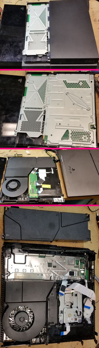
Step one is to pop the plastic case off the metal cage that holds the hard drive and slide out the hard drive, which the user can upgrade. Removing a couple of stickers on the back of the plastic case reveals the first T9 security screws, so called because they have a post in the middle. The bottom of the plastic case comes off to reveal the cooling fan, the optical drive, and the plastic case for the switching power supply. Several more security screws and Philips screws hold in these components. A metal shield then comes off to reveal the drive board for the optical drive. The optical drive, optical drive driver board, and power supply module all come out once the screws are removed and cable connectors are disconnected.
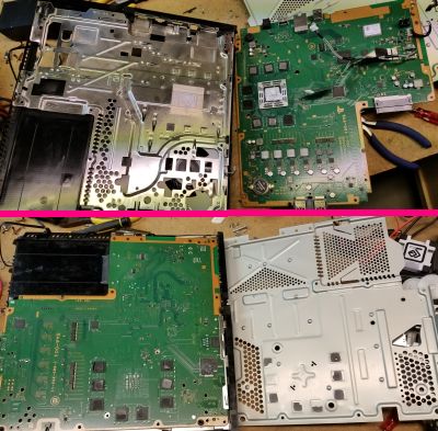
Next the top plastic lid can be pried off to reveal a flat metal chassis that provides attach points for the optical drive, power supply, fan, heatsink, and motherboard. Removing several security screws allows the metal chassis to lift out to reveal the back of the PlayStation 4 motherboard.
The heart of the PlayStation 4 is a custom-made processor chip. It clearly dissipates an appreciable amount of power because it mounts directly to the beefy metal heat sink sitting in front of the cooling fan. It is also big. Reports we’ve seen put the total chip area at 348 square millimeters, that’s a little over a half-inch square. It’s also been reported that the chip contains a graphics processor comprised of 18 compute units, in graphics processing the compute units are comparable to the cores of conventional microcontrollers. And the chip also has eight conventional CPU cores as well. The processor die has a lot of thermal paste giving a reliable connection to the massive heat sink attached to the metal chassis.
One mysterious component is a metal shield that surrounds the main processor chip. Metal shields positioned on circuit boards are usually there to prevent EMI. But this one has numerous holes in it that would limit its effectiveness as an EMI shield. So we’re guessing that it may be there to help distribute heat more evenly around the large main processor die, so one part of the die isn’t operating at a temperature that is significantly different from that of the other parts.
But though the main processor chip contains multiple GPUs and CPUs, the PlayStation 4 has other processors to handle different parts of the computational load. They are all custom chips. We found one that handles network operations carrying the SCEI label, for Sony Computer Entertainment Incorporated. You can tell it handles network processing because it sits right behind a chip from Marvell that is an ethernet controller.
Similarly, there is at least one ASIC on the board that probably assists in processing chores, but there aren’t any specific clues about what it might be doing. It sits near the ethernet processor and the connection for the optical drive.
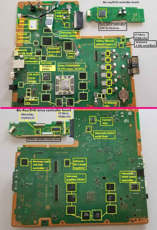
The main processor works in conjunction with a lot of memory. There are eight Samsung graphic memory chips on the main side of the board comprising four gigabytes total, and another eight Samsung chips on the other side of the board comprising another four gigabytes. These are dubbed GDDR5, standing for graphics double-data-rate five. This is a type of synchronous RAM optimized to facilitate larger frame buffers for graphically intensive computations that characterize video gaming. Also worth noting is that GDDR5 uses a total of three clocks, two write clocks and one command clock.
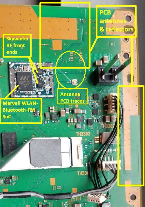
Speaking of clocks, the PlayStation 4 board contains a clock synthesis chip from IDT. It seems to be a special version, so there’s no datasheet available that we could find. But to judge by the connections on the PCB, the IDT chip probably handles clocking for the ethernet interface. There is also speculation that it has a role in synchronizing clocks for the main processor chip and the network processor because there are board traces running between the IDT chip and both processors.
In the same general area of the board as the IDT chip and network processor is a Marvell chip that handles ethernet connections. Apparently, it is the same kind of chip as on the PlayStation 3. Also in this vicinity are a couple of chips whose functions aren’t clear. One is a serial flash memory chip from Macronix. Speculation is that it serves to capture gameplay screen shots or video clips for sharing. There’s a second memory chip in the area, a two-gigabit Samsung DDR3 static RAM. This sits near the interface for the optical drive, so it’s possible it has something to do with data coming from the Blu-ray interface. The disk interface is a Genesys Logic USB 3.0 hub controller which incorporates its own eight-bit microprocessor.
At this end of the board resides the Wi-Fi module. This is a small circuit board enclosed by a metal shield that contains three main ICs. One is a Marvell WLAN/Bluetooth/FM SoC. The other two are RF front ends from Skyworks. One interesting bit about this module is that two of its antennas consist of PCB traces that can be seen on the PCB that have lengths consistent with Bluetooth and WLAN wavelengths. The third (for FM?) is a discrete wire that runs across the top of the PlayStation.
That brings us to the part of the PCB near the front panel of the PlayStation. This part holds the power circuitry that charges the remote controls, which plug into two jacks on the front panel. The main power circuits consist of six Vishay/Siliconix synchronous buck power stages. They connect to an Infineon buck regulator sitting on the bottom side of the PCB. The Infineon part seems to be generating the various power signals used by the ASICs, SoCs, etc. Powering such ICs can get to be a bit tricky because they generally use multiple power rails that must be turned on in specific sequences when the chip comes to life.
On the bottom of the PCB lies the Genesys Logic USB hub controller chip that seems to handle the remote-control ports on the PlayStation’s front panel. Rounding out the rest of the chips on the main board are an eight-bit STM MCU and Winbond 1-Mbit Flash near the remote ports. The PCB connections indicate that this processor exchanges a lot of data with the SCEI network processor. The HDMI video controller is from Panasonic and also sits on the bottom of the PCB. As well on the bottom is another custom ASIC and another Winbond serial flash chip, both near the connector for the optical drive. The serial Flash chip has connections running to the Sony ASIC chip on the other side of the board, while the custom ASIC seems to be mainly connected to the optical drive interface.
Finally, there is a temperature sensing chip from ONSemiconductor sitting near the digital/optical audio output jack. It also seems to have a connection going to this jack. This jack is used for connections to surround-sound or home theater systems. It’s not entirely clear what the temperature sensor is sensing in that it sits nowhere near any circuits that consume a lot of power.
Now to the controller board for the Blu-ray optical disk. There is one big custom ASIC made by Renesas on this board, another smaller chip whose markings we couldn’t identify, a little eight-bit MCU from STMicosystems, and a spindle motor controller chip from Rohm. Perhaps the most interesting aspect of this board is the sizable solder-stripped copper isolators it contains. One separates the STMicrosystems MCU from the rest of the board, the second sits along one of the long edges of the controller board. They are a bit mysterious. There are no high voltages circulating on this board, and the copper strips wouldn’t seem to be effective at limiting EMI because they don’t enclose anything. So we are stumped by what they are doing there.
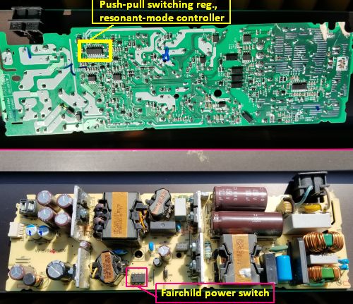
Finally, we can note a few things about the PlayStation 4 power supply and cooling fan. The power supply exhibits much simpler technology than the rest of the device. The PCB is single sided, and two main chips handle the key switching tasks. One is a Fairchild, now ONSemiconductor, chip that generates a PWM signal. One of its key attributes is an ability to throttle back in the event of low loads as a way of meeting standby and no-load energy efficiency guidelines. The other is a resonant-mode controller based on a push-pull switching regulator. The resonant-mode operation is so named because there is typically a tank circuit involved that generates a sinusoidal waveform. The reason there are two separate switching circuits is probably that the supply circuit generates two supply voltages. There are also several smaller ICs on the power supply PCB that we couldn’t identify. But most switching supplies involve the use of optocouplers as a means of getting feedback from the supply output. So we suspect that the small ICs we can’t identify may be optocouplers used for that purpose.
The cooling fan on the PlayStation 4 uses what’s called a six-pole dc brushless motor, also sometimes called an electronically commutated motors. Here commutation refers to the act of switching the electrical connection from one motor winding to the next one. The resulting magnetic field works against alternating poles of permanent magnets to generate motion. The PlayStation 4 fan motor has the magnets in its rotor. (A dc motor with the magnets in the rotor is sometimes called an outrunner. There are other possible configurations, but they are not as widely used as outrunners.)
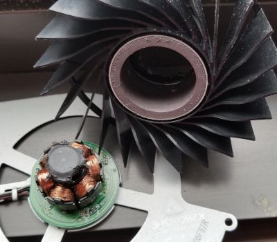
The PlayStation probably uses a brushless motor in its fan because these types are typically 85 to 90% efficient largely because most of the energy going into the coils actually moves the rotor. This is in contrast with another less expensive type of motor found in fans, the shaded pole-type induction motor. The efficiency of shaded pole motors generally is only between 15 and 30%. And the power factor is rather low as well.


Hey Lee if you could help me out I’d be appreciative. I work in a government organization where wireless signals are a big no no (secret information and spies and such). We want to add a gaming system in but it has to be vetted through our security department, i.e. they’ll check to see if any signal is emitting from the hardware. Here’s where you come in. Is it possible for you to try to remove the bluetooth/wifi module and see if the PS4 will still turn on and play without it? If it does, you’d make a military unit very happy. Look forward to hearing from you!
– Jerrod
Unfortunately, to save a few bucks, we bought a defunct unit off eBay for the teardown. So the PS4 we tore down was non-functional when we got it. Thus even if we could reassemble it, we couldn’t figure this out for you. And fyi, when we tear something down, we pretty much destroy it because we have no intention of reassembling it. Sorry we can’t help. Good luck.