If you are working with an integrated circuit (IC) and the datasheet mentions an open drain or open collector, that’s engineering speak for a current sink on an output pin. For those unfamiliar with the terminology, a “current sink” means that the current is flowing into the pin (or node, etc.), not out of the pin. (Get it? A kitchen sink drains water. In this case, a current sink drains current.) The opposite of a current sink is a “current source,” which is when the pin is driving an output current and therefore supplying current to whatever is connected to that pin. (Continuing the kitchen analogy, the current source would be the water spigot.)
Recall that a transistor is essentially an ON/OFF switch embedded in silicon. The thing that controls the transistor’s switching behavior is the base (Figure 1.) If the IC output is flowing into the base, it will switch on a flow of current through the transistor (i.e., the transistor switch is “ON.”) If there’s no flow or too little flow through IC output to control the transistor, then there is no current flow through the transistor (i.e., the transistor switch is “OFF.”) In this way, transistors control the flow of current and control voltage potentials throughout a circuit made up of hundreds to billions of transistors, depending on the IC.
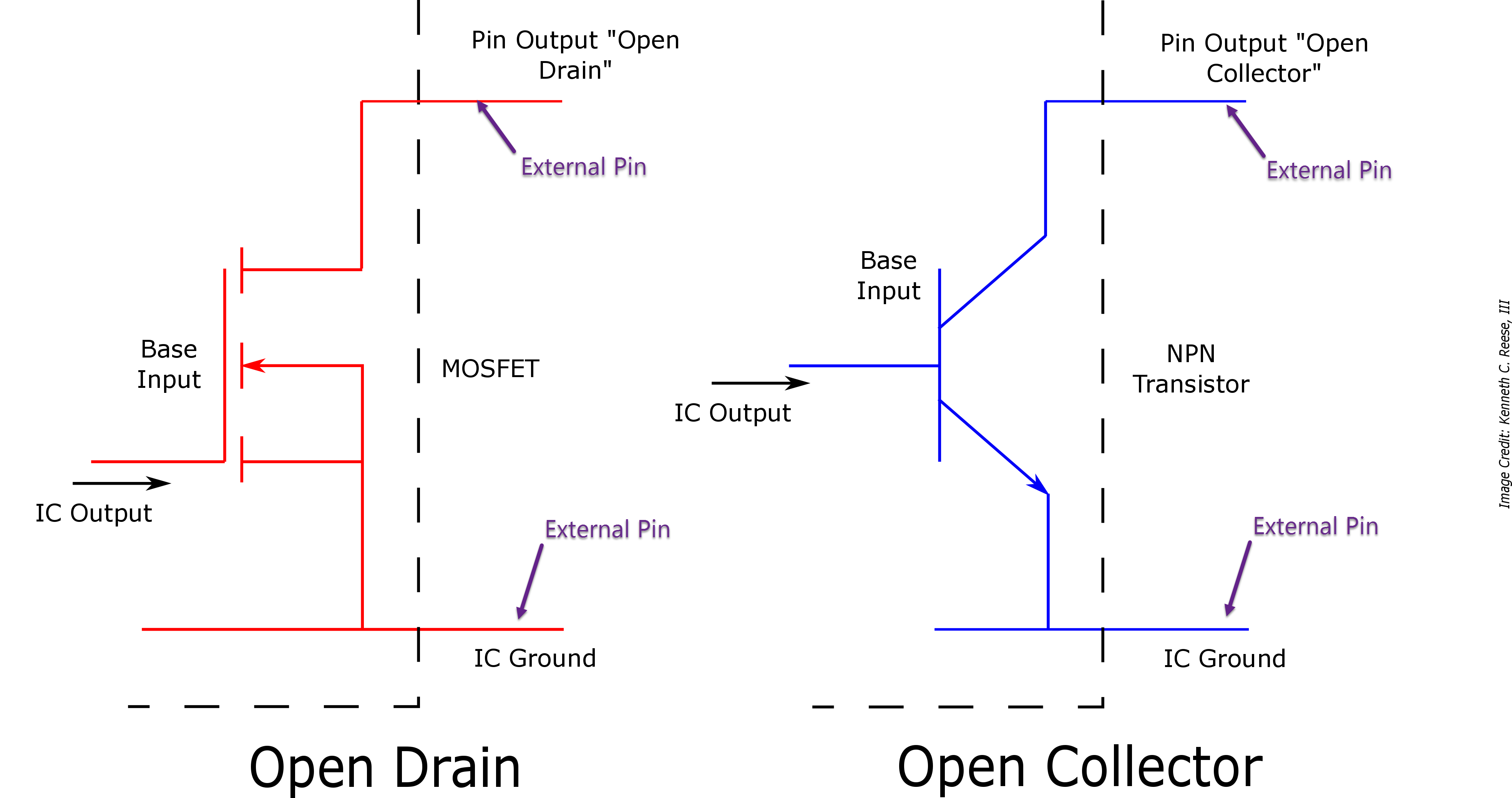
The term “open drain” means there’s a current sink, but on a FET device, for example, a MOSFET. (A MOSFET is like a transistor that can handle higher voltages but operates in much the same way.)
The term “open collector” refers to a current sink on a transistor output. If an NPN transistor is left unconnected, or open but connected to an external pin, it’s an open collector. The transistor will switch to ground when it’s active, thus “sinking” current (i.e., connecting to ground and thus current is shunted to ground for “recycling” in the ground plane). Both a current source and a current sink have current flowing but in different directions.
In both cases, the main point in the term open drain or collector is that part of the output transistor is directly brought out to a pin that is external to the IC package.
Open-collector and -drain devices sink current when controlled to one state and have no current flow (i.e., output a high impedance state) in the other state. It is fairly common to use open-drains (open-collectors) together with a pull-up resistor. The pull-up resistor is connected to high (supply voltage) at one end and connected to one or more external pins of the open-drain/-collector devices all connected together. Thus, if any one of the open-drain (open-collector) devices is set to sink current, current flow for all of the devices gets sunk to the ground, since they are all connected at the same point.
That holds the signal line high until a device on the wire sinks enough current to pull the line low. Many devices can be attached to the signal wire. If all devices attached to the wire are in their non-active state, the pull-up will hold the wire at a high voltage. If one or more devices are in the active state, the signal wire voltage will be low. Basically, the circuit has a resistor between it and the path to 5V (pull-up resistor). Pull-up resistors are used so that when the FET (transistor) is “OFF” that point in the circuit will rise to a known potential (usually it is connected to the supply voltage, but not required) rather than be left unterminated and floating at an indeterminate value, which is generally bad practice for many reasons.
The 74HC03 has a open-drain output. And as far as I can tell, no manufacturer makes a version with an up clamping diode on the outputs. If there’s no clamping diode, the pull-up resistor on the output should not have any current flowing through it. But there’s current flowing between the drain and the gate (less than a milliamp).
And I can’t find one manufacturer that specs the maximum voltage you can place on this chips output.
Thanks
You may have just not been reading the datasheets correctly. I just looked at one datasheet and quickly found the maximum voltage you can place on this chips output
The Philips datasheet for th 74HC03 states:
“In the OFF-state, i.e. when one input is LOW, the output
may be pulled to any voltage between GND and VOmax.”
In the ratings, VOmax is stated as +7V.
And that current between the drain and gate is no more than 0.5µA at 25°C, and no more than 10µA over the operating temperature range – yes, it’s less than a milliamp, more than 100 times less.
And as far as I can tell, no manufacturer makes a version with an up clamping diode on the outputs.
They wouldn’t, because the idea of an open drain rather than a CMOS output is to allow you to level-shift – e.g. from a 3.3 volt signal to a 5V TTL signal.
Thanks for the explanation!
On the last paragraph you started with “That holds”. Can you be more specific.
Thanks
F. Rahman
He’s referring to the pull-up resistor mentioned in the second last paragraph.
Scott,
pretty decent blurb on open-** devices
(What is an open drain on a FET device and how is it used?)
One comment, please edit the last paragraph.