by Jayant D’Souza, product manager Tessent group at Mentor, a Siemens Business
Charged with the task of improving yield, product engineers need to find the location of defects in manufactured ICs quickly and efficiently. Typically, they use failing test cycles to perform scan diagnosis, which is then analyzed to reveal the location and root cause of defects. Scan failure data provides the basis for many decisions in the failure analysis and yield improvement. It helps in the selection of failed devices for physical failure analysis, finds hidden systematic failures, and helps direct design and manufacturing decisions that will ultimately improve yield.
However, design sizes have been growing, a trend that is unlikely to stop. In addition to design size growth, newer processes and transistor structures present new defect modes inside the cell that require cell-aware diagnosis. Diagnosis of these cell-internal defect modes requires a diagnosis tool to complete more analysis and processing to pinpoint the location of the defect inside the cell. Performing volume scan diagnosis on today’s large, advanced node designs puts outsized demands on turn-around-time and compute resources. Product engineering teams need new techniques to manage the time and compute resources while performing ever more demanding scan diagnosis.
About volume scan diagnosis
Scan diagnosis is a well-established, simulation-based process performed on input failure log files from the ATE (automatic test equipment), along with a design netlist and scan patterns. It is used to identify and locate defects on devices that fail manufacturing test to find yield limiters, and also for field returns. Diagnosis generates a list of suspects—the suspected locations and defect mechanisms for each defect on each failed die. Statistical analysis is then applied to a population of scan diagnosis reports for failing dies. This statistical analysis applied to the population of scan diagnosis reports generates a defect pareto that shows the common root cause mechanism(s) in the population.
The memory required to perform diagnosis is proportional to the size of the design netlist. Diagnosis throughput can be increased by performing diagnosis in parallel by distributing them using a compute grid, but the efficiency of that distribution depends on the grid’s processing resources. For example, imagine a diagnosis run on a design that requires 100GB of RAM and takes about an hour for each diagnosis result. If you have 11 processors available on the grid, but only one has enough RAM to handle that job, then all the diagnosis runs will happen sequentially on that one machine, and the other 10 machines sit idle.
In terms of diagnosis throughput, which is a function of the time needed to create a diagnosis report and the amount of memory needed for the analysis, this situation is not ideal. The more diagnosis you can complete, the higher the value of diagnosis (Fig. 1). Diagnosis throughput can be improved by either reducing the amount of memory needed or by reducing the diagnosis time, or both.
Dynamic partitioning to boost throughput
There is a new technique for improving the throughput of diagnosis called dynamic partitioning. It reduces both the memory requirements and the diagnosis runtimes by intelligently reducing the input file sizes. Here’s how it works:
Often, only a small part of the design is needed in order to perform diagnosis of a fail log because a defect is activated by a specific set of patterns and the circuit’s behavior in a specific part of the design. So, a dynamic partitioning tool can analyze a fail log and create a partition that contains only the parts of the design that are relevant to that fail log. Diagnosis is then performed on this new, smaller partition.
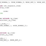
For example, say a defect in the design causes the observed values in a couple of scan cells to change, as shown in Figure 2.
These changes show up as a failing cycle on the tester, while those scan cells whose measured value matches what was expected are translated to passing cycles on the tester. The dynamic partitioning tool uses these passing and failing cycles to determine which portions of the design are relevant to the defect captured by the fail log, shown in Figure 3.
Implementing dynamic partitioning for volume scan diagnosis
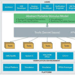
A diagnosis server on the user’s compute grid acts to automate the diagnosis flow, including partitioners that create smaller files based on the fail logs, analyzers that perform the actual diagnosis, and a monitor that coordinates between the partitioners and analyzers and intelligently distributes the diagnosis processes, illustrated in Figure 4.
The smaller input files with relevant fail log data allow more processes to be run in parallel. The number of processes that can run is limited only by the number of processors available. It also means diagnosis can run on a wider range of CPUs and deliver results faster and more efficiently than ever with no degradation in the quality of results. The partitioning process only takes a couple of minutes to complete and takes a similar amount of memory as the baseline diagnosis.
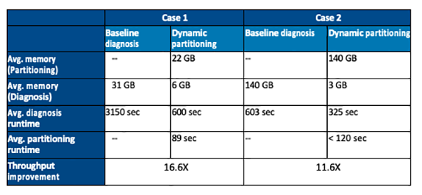
Dynamic partitioning addresses hardware resource limitations by greatly reducing the memory footprint of the diagnosis process performed by the analyzers. Through the better use of compute resources, more fail logs can be analyzed on a given day. Typically, the dynamic partitioning leads to a 5X reduction in memory and a runtime reduction of 50% per diagnosis report. The reduction in runtime translates directly to greater overall failure diagnosis throughput.
A number of case studies on real designs demonstrate the efficacy of dynamic partitioning. Table 1 shows two cases with typical improvements.
Saving time and compute resources during volume scan diagnosis can confer a competitive advantage by reducing turn-around-time, equipment costs, and improving yield faster.
Leave a Reply