Artificial intelligence (AI) and machine learning (ML) continue to push the limits of conventional semiconductor architectures. To increase speeds, lower latency, and optimize power consumption for high-performance workloads, semiconductor companies and research institutions are developing advanced photonic chips that operate on the principles of light rather than electrical currents.
This article discusses the limitations of conventional semiconductors for AI and ML, such as von Neumann bottlenecks and the slowing of Moore’s Law. It explores how engineers achieve efficiency and scalability with photonic chips, highlighting advancements from companies like Lightmatter and research institutions such as the Massachusetts Institute of Technology (MIT) and Tsinghua University. Lastly, it outlines how Lightmatter optimizes electronic design automation (EDA) workloads through cloud-based high-performance computing (HPC) solutions.
The limitations of conventional semiconductors for AI
High-performance AI and ML applications in data centers and the intelligent edge drive demand for faster, more scalable chips. In data centers, extensive training datasets, large language models (LLMs), and deep reinforcement learning (DRL) push the limits of computational power and memory bandwidth. At the edge, advanced driver-assistance systems (ADAS), wearables, medical devices, and Industry 4.0 infrastructure require increasingly complex chips to deliver rapid real-time inference within a lower power envelope, as illustrated in Figure 1.
Concurrently, research organizations are advancing artificial general intelligence (AGI) models to achieve human-level cognitive abilities. Unlike generative AI (GenAI), which creates new content, or DRL, which optimizes decision-making through trial and error, AGI will independently adapt, learn, and complete tasks without targeted pre-programming.
However, AI’s evolution is constrained by a waning Moore’s Law, limited silicon area per package, and growing energy demands in advanced compute systems. Physical limitations of CMOS technology, such as quantum tunneling effects at sub-7nm nodes, further slow miniaturization and performance gains in conventional semiconductors.
Classic von Neumann bottlenecks add to these challenges, where data transfer between memory and processing units limits performance. Larger AI models require frequent data movement between off-chip memory and on-chip compute units, increasing latency and energy consumption. Emerging solutions, such as heterogeneous architectures, in-memory computing, and photonic chips, aim to address these limitations by minimizing data movement and integrating memory and compute more closely.
Unlocking efficiency and scalability with photonic chips
Light-based photonic chips can provide a complementary and viable solution for more efficient and sustainable GenAI, DRL, and AGI workloads. Some chips perform computations in less than half a nanosecond, simultaneously executing multiple vector-matrix multiplications — a fundamental operation in neural networks. While photonic integrated circuits (PICs) generally generate less heat than conventional electronic integrated circuits (ICs), thermal management remains important, particularly for active photonic components and densely integrated designs.
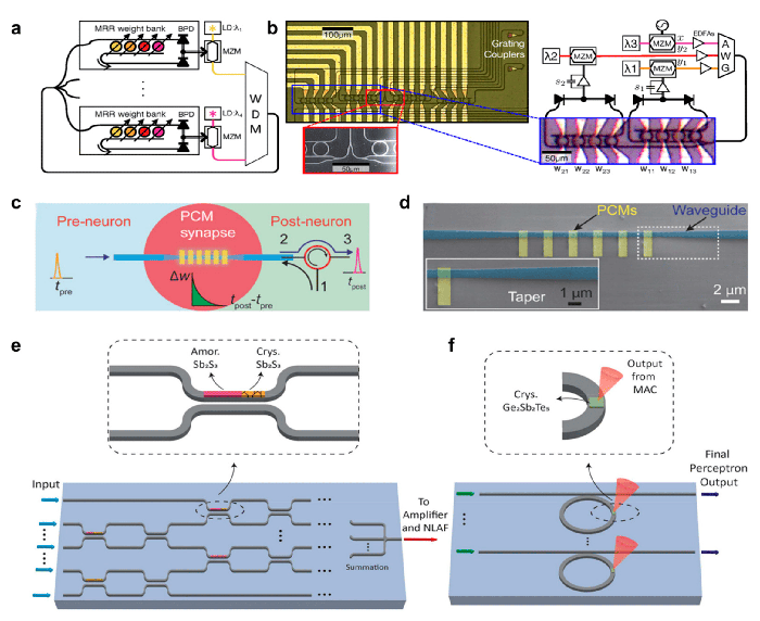
Photonic chips use wavelength division multiplexing (WDM) and ring resonators, as shown in Figure 2, to perform parallel computations across multiple wavelengths of light within single waveguides. These components enable dense information encoding and high-throughput processing, making them foundational to many photonic chip architectures. In certain designs, ring resonators are key in converting free-space optical intensity images into coherent light signals for on-chip processing, eliminating the need for separate image sensors and reducing system latency.
Photonic chips achieve high accuracy rates comparable to conventional semiconductors: over 96% during training and 92% for inference. By processing data directly using light, some photonic designs can reduce — and potentially eliminate — intermediate storage stages and the need for working memory. At the same time, advanced architectures enable in-memory or near-memory computing. These innovations reduce data movement, lower latency, and improve overall efficiency for AI workloads.
Photonic chips also excel at parallel processing on a single chip, leveraging light waves to perform multiple computations simultaneously without electrical interference.
While some photonic chip designs can be fabricated using conventional CMOS processes, many rely on specialized materials and high-precision techniques, adding to manufacturing complexity. Certain photonic chips integrate with GPU AI accelerators, enabling hybrid optical-electronic AI operations, though integration still poses significant technical challenges in many scenarios.
Scaling AI performance with emerging photonic solutions
Many research organizations and companies are advancing photonic semiconductor technology. For example, scientists at the University of Oxford demonstrated a system that uses one partially coherent light source with nine input channels to perform high-speed AI tasks at approximately 100 billion operations per second. This breakthrough has the potential to revolutionize optical interconnect technology.
Advancements in photonic chip design have enabled optical neural networks (ONNs) to execute linear and nonlinear operations entirely in the optical domain. MIT’s photonic chip integrates nonlinear optical function units (NOFUs), combining electronic and optical components to perform nonlinear operations without external amplifiers. By remaining in the optical domain until the final readout, the device enables in situ training of deep neural networks directly on-chip, delivering performance comparable to traditional hardware while operating at nanosecond timescales.
Additional emerging photonic solutions from various companies and research organizations include:
- Celestial AI: provides advanced optical interconnects for AI computing and memory infrastructure.
- ANT offers the Native Processing Unit (NPU) a PCI Express card, which delivers up to 30 times the energy efficiency of traditional CMOS technologies.
- CogniFiber: uses its DeepLight processor to deliver up to 1,000 times faster AI inference while significantly reducing cost, energy consumption, and physical footprint.
- Neurophos: combines ultra-dense, high-speed optical modulators with a planar optics stack to eliminate interconnect issues. It enables its OPU to theoretically deliver 160,000 TOPS at 300 TOPS per watt — 100x faster and more efficient than leading GPUs.
- Salience Labs: develops hybrid photonic-electronic switches for AI applications, emphasizing compatibility, reliability, and manufacturability while reducing power and cost in large clusters.
- Wave Photonics: accelerates the development of PICs across various wavelengths and platforms.
- iPronics: designs programmable photonic processors and lossless optical switches to support low-latency, reconfigurable AI architectures.
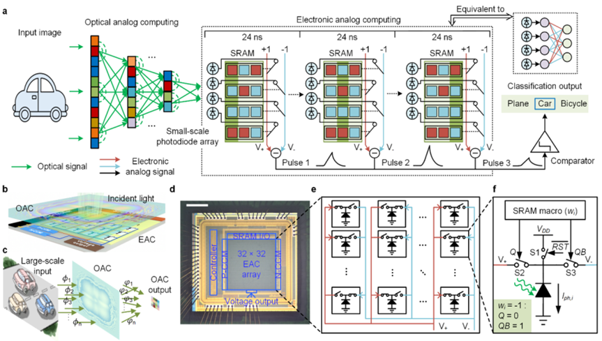
- Tsinghua University: proposes the ACCEL chip illustrated in Figure 3. This photoelectronic design uses a diffractive neural network for visual feature extraction and combines diffractive optical computing with analog electronic processing on a single integrated device.
Notably, Lightmatter is developing photonic chips with silicon-area-per-package scaling and expanded “beachfront,” enabling optical I/O across the chip area for high-performance interconnects. The company leverages advanced packaging techniques, including 3D integrating customer dies onto a silicon photonic interconnect, to connect hundreds to millions of chips in high-bandwidth, low-latency domains. Additionally, Lightmatter collaborates with GPU and switch manufacturers to support extreme scaling.
Optimizing photonic EDA workloads with cloud-based HPC solutions
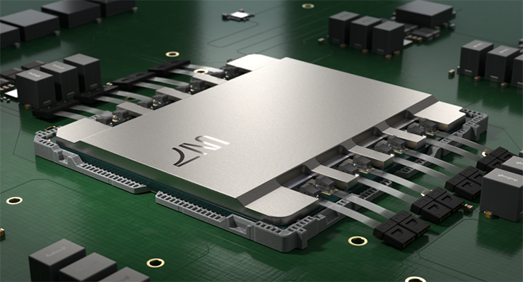
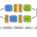
Lightmatter uses Research and Engineering Studio (RES) on AWS high-performance computing (HPC) infrastructure to streamline EDA processes for photonic chips like the one shown in Figure 4. The open-source platform enables administrators to deploy virtual desktops with pre-installed applications and tools for collaboration and data sharing.
Lightmatter also manages HPC clusters using AWS ParallelCluster and the Slurm scheduler. This setup efficiently runs parallel photonic chip simulations on remote nodes while maintaining consistent environments across local and cloud resources. Additional AWS components, such as Amazon FSx for OpenZFS shared storage and Jenkins for automated task scheduling, further bolster functionality.
Jenkins automates nightly verification, simulations, and physical design flows by detecting design changes, initiating workflows, and delivering results to dashboards and Slack channels for real-time feedback. This integrated setup streamlines transitions between small-scale and large-scale simulations and optimizes workflows across all stages of the design process.
Conclusion
Engineers are developing photonic chips that process data using light rather than electrical currents. These advancements aim to address the demands of high-performance AI and ML workloads. Photonic chips reduce latency, optimize power consumption, and improve efficiency in AI and ML applications by minimizing data movement and enabling in-memory or near-memory computing.
Related EE World content
How do Generative AI, Deep Reinforcement Learning, and LLMs Optimize EDA?
How Can In-Package Optical Interconnects Enhance Chiplet Generative AI Performance?
OFC 2024: How AI and Silicon Photonics Will Drive Network Test
Co-Packaged Optics: Higher Data Rates Increase Reliability Risks
AI, Silicon Photonics Push Networks, and Test
References
Electronic Design at the Speed of Lightmatter: Transforming EDA Workloads with RES, AWS
AI and Photonics: United by Necessity, SPIE
Startup Raises $400m to Bring Revolutionary Photonic AI Chips to Data Centers, Capacity
Photonic Integrated Circuits Benefit Greatly From AI Data Center Demand, but Other Applications Are Now Emerging, Says IDTechEx, PR News Wire
Rethinking the Computer Chip in the Age of AI, UPenn Engineering Today
Photonic Processor Could Enable Ultrafast AI Computations with Extreme Energy Efficiency, MIT
Photonic Chip Integrates Sensing and Computing for Ultrafast Machine Vision, Optica
Silicon Photonics Will Shine in the Age of AI, Electronic Design
Computer Chips Today Are Too Hot and Lightmatter Knows Why, AIMResearch


Leave a Reply