 Siemens Digital Industries Software announced that its Calibre nmPlatform now enables designers to leverage the newest GlobalFoundries (GF) silicon photonics platform. GF’s next-generation, monolithic platform, GF Fotonix is the first in the industry to combine its differentiated 300mm photonics and RF-CMOS features on a silicon wafer, delivering best-in-class performance at scale.
The GF Fotonix process design kits (PDKs) include Siemens’ Calibre nmDRC software for design rule checking (DRC) and Calibre nmLVS software for layout vs. schematic (LVS) verification. Both Calibre tools are fully certified by GF, so mutual customers designing for the new GF Fotonix platform can continue to use the trusted Calibre nmPlatform for silicon photonic devices as they have used for previous offerings.
GF Fotonix consolidates complex processes that were previously distributed across multiple chips onto a single chip by combining a photonic system, radio frequency (RF) components and high-performance complementary metal-oxide-semiconductor (CMOS) logic on just one silicon chip.
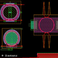
Silicon photonics enables companies to bring fibre optics directly into integrated circuits. However, silicon photonic devices contain curved layouts, rather than the linear Manhattan grid features found in traditional CMOS designs. Applying traditional CMOS DRC to silicon photonic layouts yields numerous false-positive errors that design teams must often spend weeks tracking down. To address this challenge, GF leverages Siemens’ Calibre eqDRC software, which allows rule checks to use equations in place of, or in addition to, linear measurements. This helps enable more accurate results, leading to significantly fewer errors, so design teams can spend far less time and fewer resources debugging their designs.
Similarly, the curvilinear nature of photonic structures, together with the general lack of source netlists for optics, poses a challenge when performing LVS checking. Traditional IC LVS technology extracts physical measurements from well-understood electronic structures and compares them to the intended corresponding elements in the source netlist. However, with curved structures, it is difficult, if not impossible, to discern where one structure begins and another ends. With the new GF Fotonix PDK with Calibre LVS, this obstacle is resolved with the use of text and marker layers to discern regions of interest.
Silicon photonic devices are often implemented in an individual die on a specific process node, then stacked and packaged with the rest of the design components in multiple dies using advanced heterogeneous packaging technologies. By using the complete core Calibre offering, total verification cycle times can be greatly reduced.


Leave a Reply