Hosted by Jeff Shepard
In this Virtual Roundtable session on emerging memory technologies, we are joined by Nando Basile (NB), Technology Marketing Manager for Memory with X-FAB; Bob Brennan (BB), Vice President of Emerging Memory at Micron; and Mark Reiten (MR), Vice President, Licensing Business Unit, Silicon Storage Technology (SST), a wholly-owned subsidiary of Microchip Technology.
JS: What are the important design considerations when using emerging memory technologies such as MRAM, ReRAM, etc. in applications?

NB: At X-Fab, we deal with memory specifically from an embedded perspective, rather than producing standalone memory devices. As everything is done at the die level, it must be compatible with all the other functionality that will be present in the device. We have already had a great deal of success with the implementation of SONOS into automotive ICs, shipping large unit quantities. For emerging memory technologies (like ReRAM), we are currently looking at ways to integrate this onto customers’ devices, for applications like edge computing and medical.
BB: For applications, there is a classic performance vs. capacity triangle for memory and storage technologies. At the top of the triangle is DRAM, which is optimal for latency and endurance for the most demanding volatile applications. At the base of the triangle are flash technologies (TLC, QLC), which are optimal for block storage applications. With a combination of innovative designs and massive capital investment, DRAM and NAND will continue in their roles at the top and bottom of the hierarchy for the next decade.

MRAM, such as STTRAM, has the advantage of easier integration with logic semiconductor processes. However, STTRAM has slightly higher latency and energy than DRAM with less endurance and has design implementation challenges in achieving density. As such, the industry adoption of logic + STTRAM remains to be seen. RRAM is an interesting lower latency block storage technology, and it remains to be seen if the economics of the areal density will lead to broad market deployment.
JS: Are MRAM, ReRAM, and other emerging NVM technologies ready for prime time? Are controller breakthroughs the bottleneck to enabling the growth of MRAN, ReRAM, etc.? Or is there another factor holding back growth?
NB: growth? These technologies are already starting to see traction in standalone memories, mostly because of their promising boost in density and low-power performance. In relation to embedded applications, however, they are still not totally mature, mostly in terms of technology integration and design optimization. This means that full scale embedded implementation is some way off yet, except maybe for some initial niche applications. We definitely see a lot of potential for ReRAM in the medium term – due to the low number of additional masks required, as well as with respect to its ultra-low-power performance, improved access time, and execute-in-place capabilities.
BB: There have been many credible research papers published on MRAM, ReRAM, and other technologies in conferences such as ISSCC, and these types of technologies continue to be an active research area for many semiconductor companies. Controller technologies are not holding back the adoption of new memory technologies. The greater the raw bit error rate of a memory technology, the more sophisticated the error needs to be. The lower the endurance, the more sophisticated the ASIC and the firmware need to be at managing the media. Fundamental changes to software take two Olympic cycles (eight years), and this is a major industry investment for the ecosystem to adopt a new layer in the memory and storage hierarchy.
JS: What emerging memory technologies (either volatile or non-volatile) do you expect to have the largest impact in the near-term, and where will they have the greatest use?

MR: I would like to address all three of the preceding questions at once: MRAM, ReRAM, and other emerging memories have all been emerging for a long time. These technologies all have disadvantages when compared with the Floating Gate and Charge Trapping technologies that have dominated both standalone and embedded memory products for the last 50 years.
Let’s start with MRAM. The industry has been developing MRAM for more than 20 years. The cell technology has evolved from Magnetic Tunnel Junction (MTJ) to Spin Torque Transfer (STT) architectures. The older MTJ architecture has been in production for the last decade, serving niche markets like NVSRAM replacement (Everspin) in the datacenter. No high-volume usage exists for these technologies due to product cost and inability to meet required specifications.
The STT architecture is the current approach used at advanced nodes, and it is entering production at the 28/22nm process nodes for embedded use. Both production and reliability challenges remain and are barriers to broad adoption of MRAM. The STT materials stack is comprised of 18-20 very thin layers of magnetic and dielectric materials utilizing many (Co, Ru, Mg, Fe, B, Pt) constituent elements. Depositing these layers requires atomic layer deposition, which is more expensive than other deposition techniques. Layer thickness control requirements exceed current (and any future known) in line metrology capabilities, so it is very hard to keep the process controlled, and process excursions happen more frequently as a result. The stacks are built using alternating layers of material, so etching requires a gas change to etch each layer. Gas changes take minutes per cycle, which limits the throughput to about one wafer per hour. This means an expensive etcher can only process about 20-25 wafers per day (dramatically lower throughput than other technologies). Low etch throughput and the complex, time-consuming layer deposition leads to high manufacturing costs. The stack complexity and layer thickness control (or lack thereof) lead to inconsistency and reliability issues.
MRAM has been qualified at TSMC, Samsung, and GLOBAL FOUNDRIES for production as an embedded technology at 28/22nm nodes and has gained a small following who can tolerate the cost, non-competitive specifications, magnetic field susceptibility, and other reliability constraints of the technology. This is despite the fact that MRAM is inferior to embedded floating gate technology in read speed, read/write power, and data retention. There is hope the technology can be improved over time, and the early adopters may feel they will gain some advantage if they are the first to accumulate field data for MRAM. I remain skeptical and believe these early adopters will struggle mightily and potentially fail in the market.
ReRAM has been in development for more than 15 years. It is also entering production at 28nm and also at 40nm. The main advantage of ReRAM is cost. Many different ReRAM stacks have been researched, including metal oxides (HfxOx, TaxOx, etc.), chalcogenides, and perovskites, but most of the production level work has been focused on the metal oxide materials stacks. The materials stacks are much simpler than MRAM and thus require less processing to manufacture. The disadvantage of ReRAM is even worse program/erase (Set/Reset) power, read power, read speed, and significant reliability compared to MRAM. This means ReRAM is a far cry from the industry-standard Floating Gate memories in terms of supported specifications and reliability. Regardless, TSMC is making ReRAM available on 40nm (PMIC products) and 22nm (Smart Card products) and does have some adoption for low-density applications in which the memory macro can be burdened by significant redundancy and overhead to overcome the reliability issues.
The other major difference between emerging memories and Floating Gate technologies is where in the process stack, they are implemented. Floating Gate memories are built in the front end of the process, with the device being built alongside the transistors from the substrate up. This means more process complexity but also provides significant advantages in speed and reliability. The emerging memory cells are deposited in Vias somewhere in the metal layers, which means they don’t interfere with the process front end. This has not been a differentiator so far, but on 16nm and below, where FinFet structures are used to support transistor scaling, there is much debate in the industry about the feasibility of integrating floating gate memories in the process front end. At SST, we are convinced we can do it and are engaging with major foundry partners now on evaluation of such technologies.
In summary, I believe MRAM and ReRAM will have a place in low-end microcontroller applications that don’t require high performance or high reliability, but they will not push aside Floating Gate memories now or in the future due to their limitations. I think Scotty from Star Trek said it best, “Captain, you can’t defy the laws of physics.”
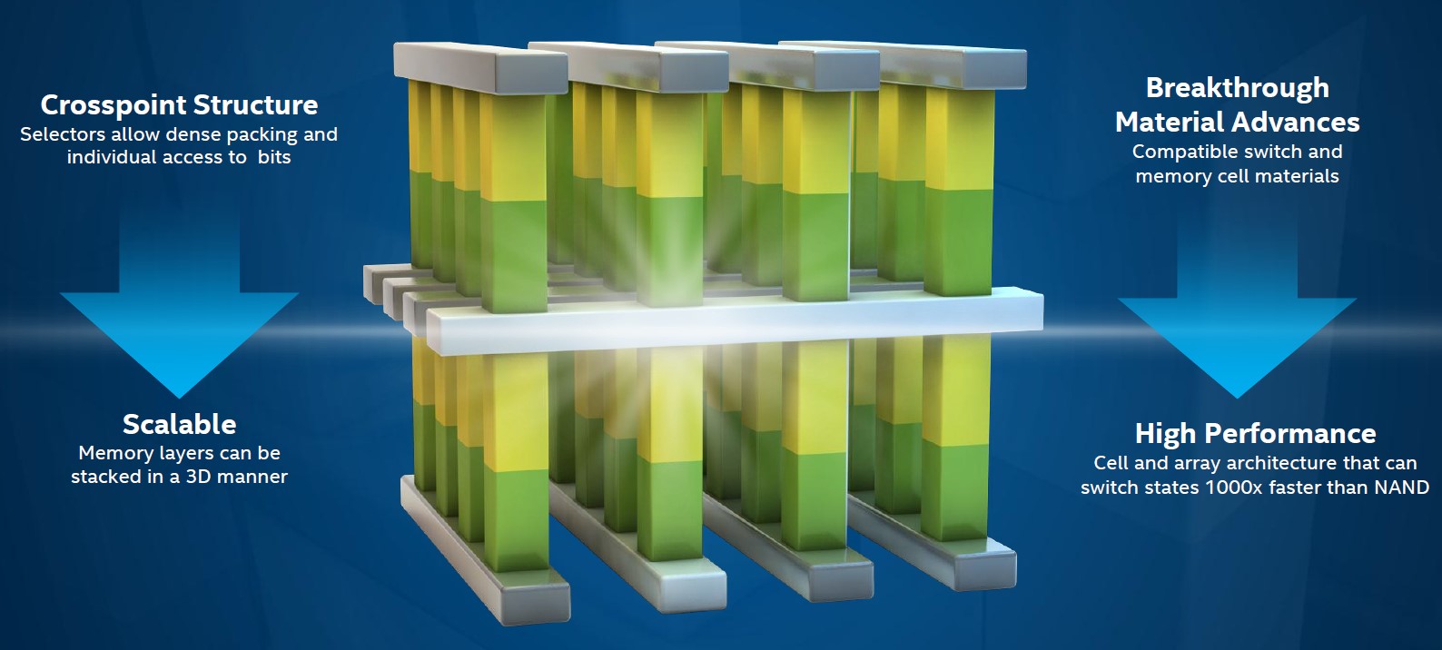
BB: Technologies such as 3D XPoint™ cross over into the non-volatile performance domain, which enables a new layer in the memory hierarchy. With up to 1,000 times lower latency and exponentially greater endurance than NAND, it enables high-speed, high-capacity data storage close to the processor. New operating systems have been written to take advantage of this layer (example: PMEM.IO), and new applications are being written to talk directly to this layer (example: DAX). These new OSes and applications will optimize their data placement in DRAM, 3DXP, and NAND to satisfy new use cases.
JS: How large of an impact do you expect to see from 3D memory technologies? At the chip level? At the package level?
NB: Though 3D stacking is already witnessing an uptake in data center, enterprise, and even consumer applications, one major concern from an automotive standpoint is how to deal with issues like thermal management (particularly ways in which to keep thermal drift under control).
BB: At the chip level, the industry has risen to the challenge of scaling flash technology with innovative 3D structures. The 3D structure of 3D XPoint™ has been well-publicized as a means to optimize both density and performance. At Micron, we are strong believers in the power of 3D memory technologies in flash and are continually innovating at the chip level to enable the technology to continue to scale.
Many exciting new 3D package technologies combine logic and memory and bring them closer together than ever before for benefits in both performance and power. One example is mobile platforms, where the tight integration of computation, DRAM, and flash have enabled small Z-heights at low thermal density, which in turn enable the increase of capabilities in an ultra-thin device.

Leave a Reply