There are many non-volatile memory technologies in use; RRAM is another option — maybe.
Random access memory (RAM), sometimes called by a more descriptive name of read/write (R/W) memory, is critical to modern electronic systems. Small amounts are needed as a numeric scratchpad or to store data samples before processing; moderate amounts are needed to store an embedded program; and huge amounts are needed for voluminous storage of just about everything and anything, such as historical data, video, images, audio, and so much more.
Non-volatile memory (NVM) stores data that can be overwritten if desired, but retains data when power is removed; in contrast, volatile RAM loses its retention when power is absent. Due to the many uses of RAM, it is available using many underlying technologies and types, including various solid-state approaches as well as electromechanical ones, such as disk drives and even “old-fashioned” tape drives (still in wide use!). Each offers a different combination of attributes to best match the application needs and priorities, such as capacity, access speed, physical size, longevity, read/write cycles, power requirements, support-circuitry complexity, and cost.
This FAQ looks at a lesser-known but commercially available RAM technology called resistive random-access memory (RRAM) or ReRAM. It is a solid-state, non-volatile memory that can be used as an independent functional block but is more often integrated in an embedded system-on-chip (SoC) for modest local memory requirements.
In brief, it works by changing the resistance across a dielectric solid-state material at its core; this core often referred to as a memristor although many industry experts don’t consider it a true memristor (that; s a discussion for another time and place). As with many solid-state and other technology devices, its functioning requires a deep understanding of solid-state physics, material science, process techniques, technology, and more.
As usual, RRAM brings the eternal innovation questions: Who even thinks of these things in the first place? Who has the persistence to pursue them to a successful conclusion? RRAM is yet another demonstration of the insightful remark by science-fiction writer Arthur C. Clarke: “Any sufficiently advanced technology is indistinguishable from magic.”
This FAQ will provide an oversight of RRAM: how it works, what it does, where it is a good fit, a little of its history, and more. It will not be a definitive exposition, but it includes links to references of varying length and technical intensity if you need more insight.
Q: What are some of its key attributes?
A: RRAM has received more attention in recent years due to its simple structure, long retention, high operating speed, ultra-low-power operation capabilities, ability to scale to lower dimensions without affecting the device performance, and the possibility of three-dimensional integration for high-density applications.
Q: What is the principle behind RRAM?
A: The device structure of RRAM is a simple capacitor-like metal-insulator-metal (MIM) structure with a switching layer sandwiched between two metal electrodes, shown in two perspectives in Figure 1. The resistance of the MIM structure can be changed on the application of a proper electrical signal, and the device retains the current resistance state until an appropriate signal is applied to change its resistance, thus representing the nonvolatile nature of the device.

Q: It seems very simple, but what’s the reality?
A: Don’t let the simplicity of the basic diagram mislead you: the reality is complicated and sophisticated.
Q: Can you provide a simple overview of how RRAM works?
A: The physical phenomenon behind RRAMs is a form of resistive switching (RS), which means that the device can be programmed into a high-resistance state (HRS, or OFF state) or a low-resistance state (LRS, or ON state) under external electrical stimuli. In RRAM, this change in device resistance is varied by the application of the external voltage pulse across the electrodes.
RRAM devices use redox (oxidation and reduction) reactions for effective data storage. These reactions form a conducting filament (CF) between the two metal electrodes within the insulator. With the application of an external electric pulse, the filament is formed between the two metal electrodes of the RRAM, and the device is said to be in the low-resistance state (logic state “1”). When the filament is ruptured, the device transitions to a high-resistance state ( logic state “0”).
ReRAM involves generating defects in a thin oxide layer, known as oxygen vacancies (oxide bond locations where the oxygen has been removed), which can subsequently charge and drift under an electric field. The motion of oxygen ions and vacancies in the oxide would be analogous to the motion of electrons and holes in a semiconductor.

Q: What are the specifics?
A: While there are several ways to accomplish the switching action, most approaches implement resistive switching in RRAM using the migration of oxygen ions in the resistive-switching layer sandwiched between the bottom electrode and the top electrode of the RRAM device. This leads to the formation of the conducting filament path. The switching mechanism of the valence change memory (VCM)-based RRAM device, showing the oxygen ion migration and diffusion, is illustrated in Figure 2.
Q: This all seems fairly intense; is it?
A: Yes, it is. Initially, during the forming process, the oxygen ions move towards the anode interface due to the soft dielectric breakdown caused by the high electric field, leaving behind oxygen vacancies in the resistive switching layer. Thus, defects are generated, which results in the formation of CFs. For the transition of the memory cell from LRS to HRS, the reset process occurs during which the oxygen ions migrate back to the bulk to recombine with the oxygen vacancies.
The resistance switching in VCM-based RRAM devices can be modulated by further tuning the initially formed conductive filaments by controlling the magnitude of the external electric field applied. A flow diagram depicting the operating mechanism of the RRAM is shown in Figure 3.

Q: Can you provide more details on the physical sequence?
A: The sweeping sequence of the switching stages of RRAM is shown in Figure 4.

Q: A single memory bit is interesting but not useful—what about memory arrays?
A: How to do that is one of the issues associated with RRAMs. What is known as a one-transistor, one-resistor (1T1R) architecture is preferred in some ways, because the transistor isolates current to cells that are selected from cells that are not. On the other hand, a cross-point architecture is more compact and may enable vertically stacking memory layers, ideal suited for mass-storage devices. There are many performance, consistency, manufacturability, and support-circuitry issues related to choosing and fabricating a viable array.
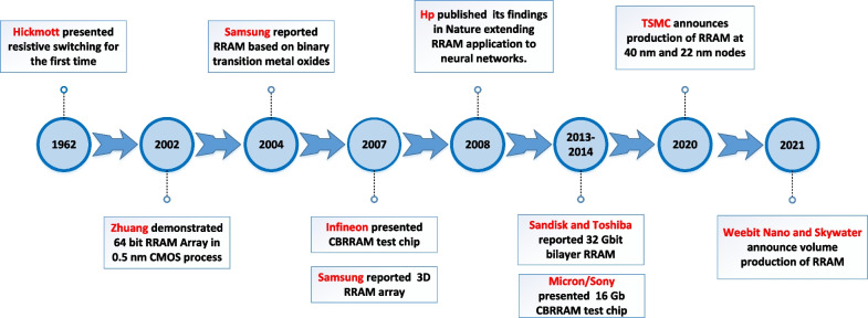
Q: What’s the history of RRAM development?
A: As is generally the case, these types of advances have a long gestation period, from “is this even possible?” to actual working model and then to commercial versions. Some of the initial conceptualization and experimentation were done in the 1960s.
However, this effort was largely unnoticed until Hewlett-Packard — the leading test-and-measurement company at the time, before it divested its T&M division and split into an “enterprise software” company and a hardware provider — developed a device called a memristor and promoted it as the “next big thing” in memory technology. Their publicity led to renewed interest and eventually to RRAM devices, as seen in the timeline of Figure 5.
Q: Are RRAMs used in any standard products?
A: While RRAMs have not yet lived up to the promise (or hype) of its proponents, there is some commercialization. For example, Infineon maintains that RRAM outperforms traditional NOR Flash, EEPROM, and magnetic RAM solutions and enables advanced AI/ML in so-called “edge” devices. They offer a microcontroller family with RRAM for NVM roles.
Among the reasons they cite is that embedded systems need long-term reliable memory for boot code, and RRAM provides 20 years of data retention, along with radiation and magnetism tolerance. Applications such as data-logging are characterized by high-repetition writes of small amounts of data. RRAM’s high endurance and byte-granular writes support the vast majority of these workloads, demonstrating the versatility of the memory.
Infineon RRAM memory cells utilize a metal-oxide switching material and are designed in a one-transistor one-resistor (1T1R) configuration. Switching energy is low, switching speed is fast, and endurance is high. The memory is manufacturable using standard CMOS fabrication processes, and is proven to be scalable below 30 nanometers.
Infineon further notes that a key benefit of RRAM, as compared to NOR Flash architectures, is driver-design simplicity for two reasons. First, the RRAM technology does not require an erase command before rewriting to memory. Second, it also supports byte-granular writes as opposed to NOR’s page-level write commands. Fewer commands and memory operations also contribute to RRAM technology’s inherent power, performance, and endurance advantage.
Q: Are there other products that use embedded RRAM?
A: Yes, the Nordic Semiconductor nRF54L family of wireless system-on-chip (SoC) devices integrates an ultra-low power, multiprotocol 2.4-GHz radio with a microcontroller, featuring a 128 MHz Arm® Cortex®-M33 processor, seen in Figure 6. The SoCs include 500 kilobytes (KB) to 1524 KB RRAM-based non-volatile memory (depending on specific version) in addition to 96 KB to 256 KB of “conventional” RAM.

Q: If RRAM has so many virtues, why hasn’t it achieved greater success?
A: There is no simple, single answer to a question such as this. The answer depends on the priorities of prospective users and the tradeoffs they are willing to make, along with fabrication considerations at the vendor.
A complete RRAM subsystem involves balancing and prioritizing tradeoffs in design complexity, scalability to perform at higher memory densities, power requirements, manufacturing consistency versus memory size, longevity, performance versus temperature swings, long-term reliability, footprint on the chip, and cost. As in most design scenarios, there is no single right or best answer.
To date, RRAM has only been successful in some well-defined niches. That could change, of course, and there have been many cases of a technology that wasn’t yet “ready for prime time” but was always in second place, until a combination of developments changed the situation. We’ll have to see how it works out for RRAM in the next few years.
Related EE World content
Perfectly Formed Random-access Memory
Stanford Engineers Find That A New Memory Technology May Be More Energy Efficient Than Previously Thought
Data Use Draining Your Battery? Tiny Device to Speed up Memory While Also Saving Power
Three-Dimensional Chip Combines Computing And Data Storage
‘Memristors’ based on transparent electronics offer technology of the future
SoCs support security requirements, AI/ML, and HMI for next-gen applications
References
Resistive Switching Random-Access Memory (RRAM): Applications and Requirements for Memory and Computing, ACS Publications (very long but very useful)
Resistive random access memory: introduction to device mechanism, materials and application to neuromorphic computing, NIH/National Library of Medicine (very long but very useful)
EE Research Talk—Next generation memory technology: a Resistive Random-Access (ReRAM) Memory, University of Washington/YouTube (52-minute video, very useful)
Resistive Randon-Access Memory, Wikipedia
RRAM or ReRAM (resistive random access memory), TechTarget
RRAM Resistive Ram, Infineon
Flash Forward: MRAM and RRAM Bring Embedded Memory and Applications into the Future, Synopsys


Leave a Reply