![]() Xperi Holding Corporation and Tower Semiconductor announced Tower’s license of Invensas ZiBond and DBI 3D semiconductor interconnect technologies. This technology complements Tower’s manufacturing of its state of the art stacked wafer BSI sensor platforms for time of flight (ToF), industrial global shutter and other CMOS image sensors on 300mm and 200mm wafers. In addition, Tower Semiconductor will explore the use of Invensas enabling 3D integration technologies for a broader range of applications, including memories and MEMS devices.
Xperi Holding Corporation and Tower Semiconductor announced Tower’s license of Invensas ZiBond and DBI 3D semiconductor interconnect technologies. This technology complements Tower’s manufacturing of its state of the art stacked wafer BSI sensor platforms for time of flight (ToF), industrial global shutter and other CMOS image sensors on 300mm and 200mm wafers. In addition, Tower Semiconductor will explore the use of Invensas enabling 3D integration technologies for a broader range of applications, including memories and MEMS devices.
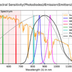
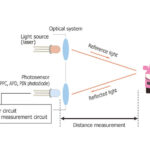
With the recently released full design kit for hybrid bonding, Tower’s customers can now design their products on two different wafers, an imager wafer and a mixed-signal CMOS wafer, that are then stacked together with electrical connections on a pixel level, from 10um pitch for applications such as Direct ToF (dToF) and event-driven sensors, down to 2.5um and even below for applications such as mobile ToF for face recognition applications. This separation into two wafers allows very high-speed circuitry on the CMOS side, with very high sensitivity pixels, due to backside illumination, and extremely low dark current, below 1 electron/sec per square micron at 60 degrees Celsius, on the imager side. Tower’s unique platform also allows the use of different Epi thicknesses for near-infrared sensitivity enhancement.
![]() Industry momentum is building around 3D semiconductors that are smaller, thinner and higher performance to enable a new wave of applications for automotive, industrial, Internet of Things, edge computing and consumer device markets. Invensas has achieved fundamental advances in the semiconductor packaging and interconnect technologies required to create 3D stacked chips that satisfy demanding size and performance requirements. Invensas ZiBond direct bonding technology and DBI hybrid technology are ideal for high-throughput, low cost-of-ownership fabrication processes.
Industry momentum is building around 3D semiconductors that are smaller, thinner and higher performance to enable a new wave of applications for automotive, industrial, Internet of Things, edge computing and consumer device markets. Invensas has achieved fundamental advances in the semiconductor packaging and interconnect technologies required to create 3D stacked chips that satisfy demanding size and performance requirements. Invensas ZiBond direct bonding technology and DBI hybrid technology are ideal for high-throughput, low cost-of-ownership fabrication processes.


Leave a Reply