Three of the keys to successfully managing power consumption and dissipation in embedded systems are using various active power management techniques, power-aware code, and software optimization, and making power management an integral part of the design flow process from the beginning.
Active power management can include the use of power gating, clock gating, dynamic voltage scaling, and adaptive voltage scaling. Power gating involves putting circuit blocks and subsystems that are not currently being used in standby. It is one of the simplest forms of active power management. Implementation of power gating involves balancing the amount of energy saved by using standby for a particular block with the energy consumed to start and stop the block’s operation. Power gating is typically implemented using a combination of hardware and software control.
Memory systems are often a candidate for power gating. In the case of power gating memory blocks, the amount of energy saved varies based on each application system’s usage patterns. For example, with non-volatile memories, the write power is typically much higher than the read or standby power. That means that write times need to be minimized in power critical designs, especially in systems that require frequent writes to memory.
The power-up time for the specific memory being used is a critical consideration for power gating. Memories with faster power-up times can be placed into standby more frequently. A second important consideration is the leakage current when in standby mode. The higher the standby leakage current, the less the benefit from power gating.
While power gating aims to reduce the leakage power in a circuit, clock gating aims to reduce dynamic power. Clock gating removes the clock signal when the circuit is not in use. Clock gating saves power by pruning the clock tree, at the cost of adding more logic to a circuit. Pruning the clock disables portions of the circuitry so that the flip-flops in them do not have to switch states. Switching states consume power. When not being switched, the switching power consumption goes to zero, and only leakage currents are incurred.
Voltage scaling
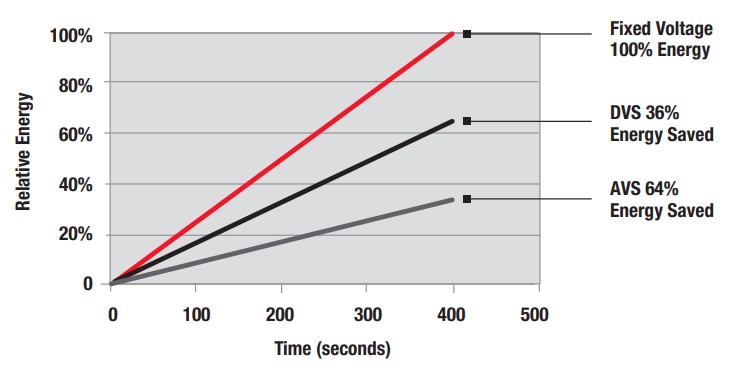
Voltage scaling is typically implemented in one of three ways; dynamic voltage scaling (DVS), dynamic voltage and frequency scaling (DVFS), and adaptive voltage scaling (AVS). AVS is a closed-loop dynamic power minimization technique. AVS allows the voltage supplied to the chip, and therefore its power consumption, to be continuously adjusted to be appropriate to the workload and the parameters of the specific chip. This is accomplished by integrating a device that monitors the performance of the chip (a hardware performance manager) into the chip, which then provides information to a power controller.
AVS is similar in its goal to DVS and DVFS. AVS provides greater power savings compared with DVS and DVFS, which are open-loop techniques. All three approaches aim to reduce power usage and heat generation. AVS adapts the voltage directly to the conditions on the chip, allowing it to address real-time power requirements and chip-to-chip variations and changes in performance that occur as the chip ages. The advantages of AVS include:
- Delivery of the desired voltage to every block of the system despite variations in temperature, process corner, and frequency;
- Processor- and architecture-independent implementation of power reduction;
- Typical savings of about 55% compared to open-loop Dynamic Voltage Scaling approaches.

Performance implications of AVS
The use of AVS has device performance implications that need to be considered by designers. For example, in battery-powered systems with an input voltage of 3.6V, it may be most efficient to power internal logic and flash memory using a high-efficiency dc/dc converter. As the battery discharges and the battery voltage declines, it can be more efficient to power the flash and internal logic from different sources because the internal logic can operate at lower voltages than the memory. For example, the SiM3LK1xx low-power 32-bit MCU family from Silicon Laboratories has a flexible power architecture with six separate and variable power domains that enable dynamic optimization.
CMOS logic circuits typically operate more slowly at lower input voltages. If the application can tolerate lower performance, then reducing energy consumption using AVS and a lower voltage can provide substantial energy savings. Leakage provides a lower limit on the effectiveness of AVS. For example, if a particular function takes too long when performed with a lower voltage, leakage will begin to dominate the energy equation and increase overall energy consumption. In these cases, it can make sense to execute a function as quickly as possible (at a relatively higher voltage) and then put the processor into sleep mode to minimize the leakage component.
Power-aware code and software execution optimization
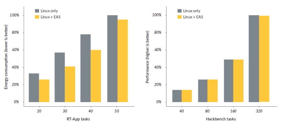
Energy-Aware Scheduling (EAS) is an enhancement to Linux power management, placing CPU power control directly under the Linux scheduler. When enabled, EAS uses the task load and a CPU Energy Model to select the most efficient CPU to run on, taking advantage of the power and performance of Arm big.LITTLE and Arm DynamIQ-based systems. EAS is tightly connected with the Linux DVFS subsystem. EAS is merged into upstream Linux as of kernel v5.0 and later.
The figure below shows test results using EAS on an Arm Juno r0 platform using RT-App (a synthetic workload generator) in a low-intensity scenario where energy consumption is the primary concern and using Hackbench as a performance benchmark.

Power-aware verification
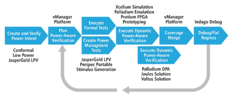
Power-optimization techniques are creating new complexities in the physical and functional behavior of electronic designs. An integral piece of a functional verification plan. For example, Cadence offers a power-aware verification methodology that can help verify power optimization without impacting design intent, minimizing late-cycle errors and debugging cycles.
The methodology brings together power-aware elaboration with formal analysis and simulation. With power-aware elaboration, all of the blocks and the power management features in a design are in place so that designers can verify the design with power intent. Power intent introduces power/ground nets, voltage levels, power switches, isolation cells, and state retention registers. Any verification technology—simulation, emulation, prototyping, or formal—can be applied to a power-aware elaboration of the design.

The integration of code scheduling, power gating, adaptive voltage scaling, and power-aware code can increase energy savings and lower dissipation in embedded systems.
This was the first article in a three-part FAQ series on various aspects of embedded system design. The second article will consider securing embedded systems in a hostile world. The third and final article in this series will look at embedded systems software and programming for a safer world.
References
Adaptive voltage scaling, Wikipedia
Adaptive voltage scaling technology, Texas Instruments
Designing Low-Energy Embedded Systems from Silicon to Software Part 2 – Software Decisions, Silicon Laboratories
Energy Aware Scheduling (EAS) in Linux 5.0, arm
Power-Aware Verification Methodology, Cadence
Power gating, Wikipedia


