Identifying the components reveals clues as to how a graphics card works, assuming you can read the identifying marks and find documentation.
Wandering through an electronics swapfest, I found someone selling a graphics card and wondered what was inside. I bought it for $20, opened the case, and looked up the architecture and components.
Released in December 2011, the AMD Radeon HD 7970 GPU card was at the time considered a high-end graphics card for gamers. Today, not so much. Even so, there’s plenty to learn from this card. You can find many reviews of this card, though most approach it from a user’s perspective. Users don’t care what makes this board run other than to make sure their power supply is up to the task. The reviewers tested the graphics card by running games on it and looking at how the card performs. Engineers take a different approach. That’s not to say that all reviews look exclusively at the gamer’s experience. Some reviews test the card for power consumption and cooling.
Removing the cover reveals a massive heat sink, which is mechanically and thermally attached to the GPU — I’ll cover that later. Looking at the board in Figure 1 with the heat sink and GPU removed, you can see that it contains three major sections: DC-DC converter, compute (GPU and 3 GB of memory), and external I/O (DVI, HDMI, 2x DisplayPort). The fingers at the top left let you daisy-chain additional cards. Of course, there’s a PCIe 3 set of fingers for 16 lanes.

Graphics cards produce considerable heat and the Radeon HD 7970 requires two PCIe slots. Table 1 below covers the basic specs of interest to users.
Table 1. Radeon HD 7970 graphics card specifications
| Component | Description |
| GPU | Tahiti XT (215-0821060) AMD Radeon HD 7970 GPU (215-0821060) |
| Memory | 3 GB GDDR5 |
| Memory interface | 384 bit |
| Core clock | 925 MHz |
| Boost clock | 1050 MHz |
| Memory clock | 5500 MHz |
| Cooler | IceQ X² |
| Outputs | 1x DVI, 1x HDMI, 2x Mini DisplayPort |
| Bus interface | PCIe 3.0, 16 lanes |
Power section
The DC-DC converter takes 12 V from the system power supply and drops the voltage while increasing the current. The capacitors in Figure 2 are 820 µF, 2.5 V. I’ve not found any specs that verify the operating voltage, though some reports put it at 0.85 V.

The heart of the DC-DC converter is a CHl8225G eight-phase PWM buck controller (Figure 3). It controls eight phases, though the graphics card uses six phases with an additional set of unpopulated PCB pads, presumably for powering future variants. The controller drives six pairs of power transistors, each pair through an IRF3537/CHL8510 12 V gate driver mounted on the back of the board directly under the transistors, which appear in Figure 4. Each pair of transistors drives numerous components, most notably an FP1007R3-R15-R, 150 nH high current, high-frequency power inductor in Figure 2.

The transistor pairs in Figure 4 consist of 25 V single N-channel IRF6894 power MOSFET and Schottky Diode in a DirectFET MX package rated at 33 A. The smaller transistor, marked 68114A, appears to be from IR (Infineon) but didn’t appear in any search. If you know more about this device, please post a comment. The larger transistor cases connect to ground, confirmed with an ohmmeter.

How much power does the buck converter deliver to the load, which consists of the GPU and 12 Hynix H5GQ2H24 AFR 2 Gbit (64Mx32) GDDR5 SGRAM parts? Several reviews of the card suggest that the Radeon HD 7970 consumes 250 W. One review said the card “guzzles down 254 W” and recommended a 500 W power supply for any computer running this card.
Computing section
The total GPU memory is 24 Gbits, 3 Gbytes. Figure 5 shows the GPU and memory on the board. Figure 6 shows a close-up of a memory device. The back side of the PCB holds a set of resistors and capacitors mounted directly underneath and aligned with each memory IC’s orientation.


The GPU, designated U1, is surrounded by decoupling capacitors. A few dozen reside on the substrate where the IC is mounted, while more than 100 reside underneath the GPU on the back of the PCB shown in Figure 7. A few dozen more capacitors reside in the surrounding area.

Digital ICs need clocks, and the 7970 GPU is no exception. Near the lower left corner of the GPU is a Silicon Labs SL16020DC low-power dissipation spread-spectrum clock generator (U5) connected to a 27.000 MHz crystal.
Continuing down and to the right, we find the 300 section of components and U3, an AIMC A25L010 256 kbyte flash memory. A second A25L010 (U2) is located on the back of the PCB. The flash memory contains the GPU BIOS.
U300, a uP1509P supplies power to the flash memory, which has a voltage range from 2.7 V to 3.6 V. I was unable to find any documentation on my own, so I queried people at Electro-Tech-Online for help. One person replied with a link to a Ukrainian website containing a photo of a part identical to the one on the PCB. That page led me to an application schematic. Another person suggested that the part could be an XL1509, a 2 A buck DC-DC converter. The XL1509 datasheet says that the device can provide 3.3 V, 5 V, and 12 V, of which 3.3 V could support the flash memory. Using Microsoft Copilot to translate the Ukrainian, I found that the uP1509P is a 0.85 V CPU power controller. That’s consistent with the 0.85 V GPU operating voltage. Your thoughts? Leave a comment.
The back side of the board contains more parts in the 300 series. Given the 2.2 µH inductor L301, they are surely power-related. Given their proximity to flash memory U2 (Figure 8), we can assume they are part of its power circuit.

Figure 8 also shows U1501, a 74HCT125 quad 3-state buffer manufactured by several companies, including Texas Instruments, Diodes Inc., and NXP. Given its 1500-series designation and proximity to a DVI video connector, we can conclude that U1501 supports that function.
More DC converters
On the front of the board, just behind the DVI connector, resides another power circuit, shown in Figure 9. Here, we find a classic 7805 linear regulator, designated U400. Close inspection shows that the 7805 ground pin has been cut. Figure 10 clearly shows the cut lead. That’s neither a mistake nor tampering because the regulator’s ground connection on its back does connect the regulator to ground. Indeed, a datasheet showing the TO-252 package reveals the regulator’s ground connection is cut at the factory.

Another power-supply section, the 900 series of components located above the 400 series and just behind the DisplayPort connectors, appears in Figure 11. It’s a switching regulator. Inductor L900 is misaligned. That’s possibly a manufacturing defect but not enough to cause the board to fail. A corner of the case is, however, slightly chipped when viewed with the magnifier. Thus, it’s possible that the inductor was replaced, but I can’t rule out the board passing QC as long as it passed manufacturing tests.

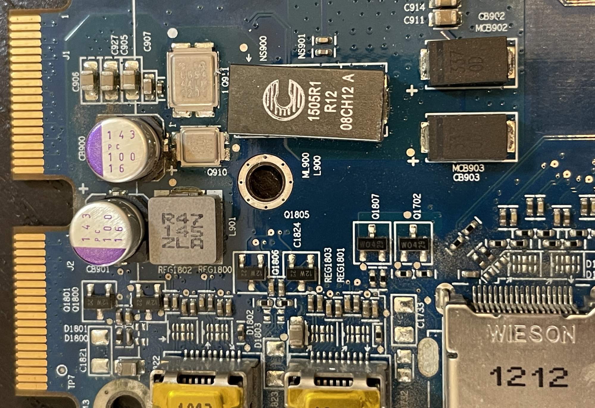
Note the pair of diodes where the one marked CB902/MCB902 is slightly misaligned. Is this another manufacturing defect not serious enough to cause a failure?
Cooling
We’ve discussed the main power section, which delivers about 250 W. Now, let’s look at the heat sink shown above the board in Figure 12. Fifteen large holes on the board shown in Figures 8 through 11 align with threaded inserts in the heatsink/fan assembly. Those inserts accept screws in the final assembly. As you’d expect, the large holes are also vias that connect to ground and transfer heat from the board to the heatsink. An article in Tom’s Hardware discusses the power draw and temperature of the Radeon 7970 graphics card, comparing it to its competition at the time of its release.

Observations
The AMD Radeon HD 7970 graphics card was a powerhouse in its day. A look inside shows how much power-electronics engineering went into it. The board layout separates the main power converter from the GPU and memory, which consumes most of the 250 W needed to power the card. Much smaller power circuits handle the video ports, PCIe interface, and I/O bus for connecting multiple GPU cards. Heat dissipation requires a large heatsink combined with lots of paths to pull heat away from the board.
Perhaps the most difficult part of this project was reading the markings on the components. Armed with an over-the-head magnifier with an LED let me read those tiny letters and numbers. Even with that, reading the print required tilting the board to just the right angle for the light to illuminate each part. Then came the parts search, which required two search engines, an AI assistant, and finally, asking the Electro-Tech-Online community. Still, a few parts remain unidentified.


It’s common in AMD designs to use something like 74HCT125 gates as buffers for the HSYNC and VSYNC for the VGA output part of the DVI-I connector. Also could be used as a buffers for the HPD pin for DVI and HDMI. It’s not usually a good idea to connect sync and HPD directly to the graphics chip as transitions can blow it up.
I brought the board to APEC to ask power electronics engineers about the design. Several said that today’s boards need so much more port that the can;t be designed with the power section so far from the GPU. Instead of surrounding the GPU with memory, today’s graphics cards have the the power electronics surrounding the GPU on both the top and bottom sides of the board.
Regarding the buck converter in Figure 3, CHIL is now part of Infineon.