Differential signaling is a way of transmitting a signal using two conductors that carry equal-magnitude, opposite-polarity waveforms, and the receiver measures the voltage difference between them rather than referencing a common ground.
This article discusses the physical properties, circuit mechanics, and system-level implementation requirements of differential signaling.
The fundamental physical properties of a high-speed differential signal
Differential signaling transmits complementary signals over two conductors, typically designated as the A-wire and B-wire. These signals consist of high-speed pulses with equal amplitude but opposite phase. For a receiver to accurately recover data, the pair must maintain electrical symmetry and consistent impedance.
As shown in Figure 1, a primary requirement is maintaining a consistent odd-mode impedance (ZODD) when both wires are excited differentially. Impedance fluctuations along the length of the pair cause signal reflections, which degrade the waveform.
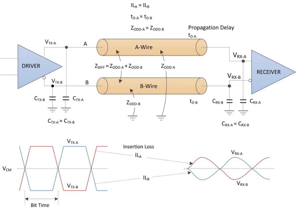
Timing is also important for data recovery. The propagation delay (tD) and insertion loss (IL) of each wire must be matched. If the signals do not arrive at the destination simultaneously, the complementary timing is compromised, leading to increased jitter and a reduced eye opening. This degradation directly impacts the bit error rate.
How do LVDS circuit mechanics manage EMI and noise?
Generating these waveforms requires specific driver and receiver architectures. Low-voltage differential signaling (LVDS) is a standard implementation that uses a current-steering approach rather than voltage-rail switching.
An LVDS driver (Figure 2) uses a constant-current source, typically 3.5 mA. The receiver is designed with high dc input impedance, causing the driver current to flow through a 100 Ω termination resistor at the receiver. This results in a controlled, low-amplitude voltage difference of approximately 350 mV. This low-voltage swing enables high data rates while maintaining stable power consumption across different frequencies.
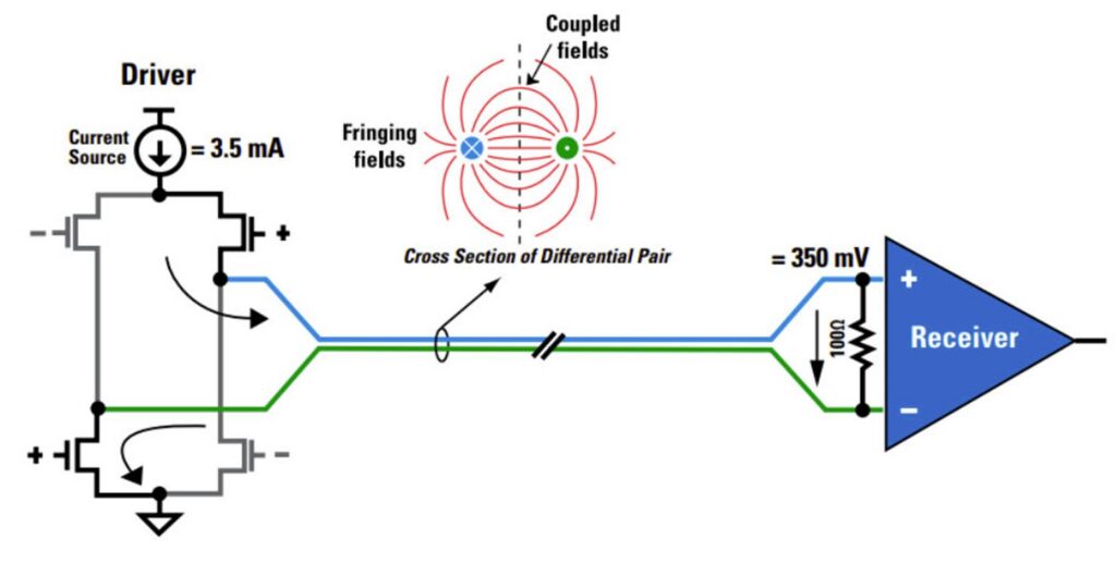
As illustrated, this architecture provides two primary electrical advantages:
- Common-mode noise rejection: External noise often couples onto both conductors of the differential pair equally. Because the receiver detects only the difference between the two signals, this common-mode noise is mathematically canceled.
- EMI suppression: The magnetic fields generated by the equal and opposite currents in the A and B wires cancel each other out. The coupled and fringing fields shown result in lower electromagnetic radiation compared to single-ended signaling.
System-level constraints required for a balanced interconnect
System-level performance depends on the interconnect’s physical implementation. Figure 3 illustrates such an arrangement. A standard differential transmission system consists of a host controller, a transmitter (such as the SN65LVDS31), a balanced interconnect, and a receiver (such as the SN65LVDS32).
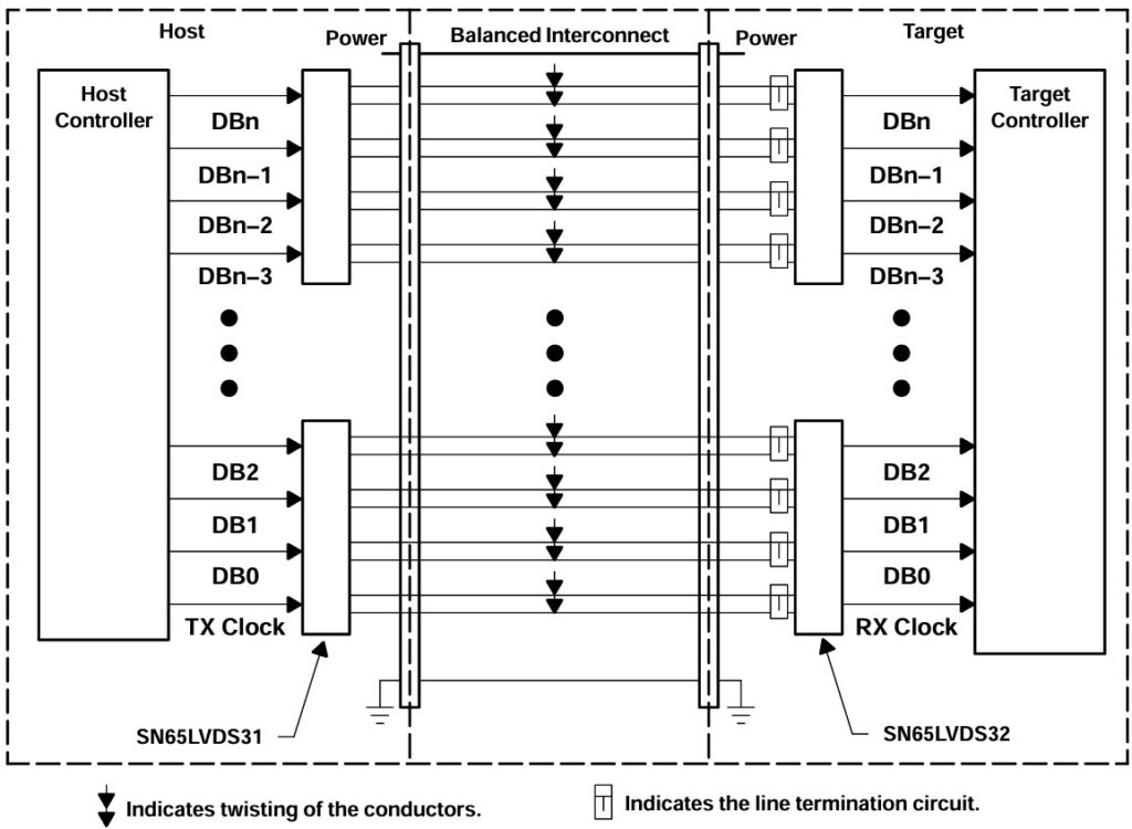
Signal transition times can be as short as 260 ps. At these frequencies, PCB traces function as transmission lines within a few centimeters, requiring specific routing protocols:
- Controlled impedance: Traces must maintain a differential impedance near 100 Ω. This is achieved through a specific PCB stack-up design, including symmetrical dielectric thickness and appropriate trace geometry.
- Trace length matching: The physical length of each trace in the pair should be matched, typically within 5 mm. Designers use mitering or serpentine routing to ensure identical propagation times.
- Balanced interconnect media: While twisted-pair cables are common for their uniform coupling, any balanced medium must maintain a consistent distance between conductors.
- End-of-line termination: As indicated by the termination circuits in Figure 3, a resistor (typically 100 Ω, as detailed in Figure 2) must be placed at the far end of the transmission line, as close to the receiver inputs as possible. Proper termination prevents signal reflections that would otherwise interfere with data sampling.
Summary
Implementing high-speed differential signaling involves a focus on electrical symmetry. By using LVDS mechanics to cancel common-mode noise and suppress EMI, systems achieve high data rates with stable power consumption. Hardware selection is one component. Precise PCB layout, controlled impedance, and far-end termination are necessary to preserve signal fidelity across the interconnect and ensure consistent system performance.
References
ELEX3525: Data Communications – Differential Signalling, The University of British Columbia
Applications of Low-Voltage Differential Signaling (LVDS) in LED Walls, Texas Instruments
Low-Voltage Differential Signalling – Design Notes, Texas Instruments
Differential Pairs: What You Really Need to Know, Texas Instruments
EEWorld Online related content
Understanding single-ended and differential communication systems
Reducing ringing or reflections by controlling impedance lines
Understanding the basics: What is characteristic impedance?
Sorting out balanced cables and differential signaling
Making measurements on balanced transmission lines
Testing LVDS devices at the margins with an AWG

Leave a Reply