A Printed Circuit Board (PCB) layout, in its most basic form, is a means to transfer a circuit from a breadboard to a more stable and permanent physical form. Whereas entire books and college coursework have been dedicated to PCB layout, what follows is a short overview of what to consider when making a PCB.
Schematics
Start by creating a great schematic, since the schematic is both the primary documentation and the map for understanding and constructing a system of circuits. A schematic is a diagram of circuits, components, and connections that are laid out in a manner that is easy to follow. Components and connections between components (or netnames) are clearly identified. A great schematic includes as much information as possible, including tolerances and sizes, notes on thermal issues, tuning procedures (if any), placement of critical components, information for a PCB (e.g., board stack up), recommendations on controlled impedance routing, component de-rating, and perhaps a sequence of operations (if the schematic is not already part of a manual). Notations on the schematic are encouraged. Do not assume that everyone who subsequently reads the schematic will know as much as you, or the same things as you do.
High-frequency signals
PCBs that support high-frequency signals have special requirements. Generally, you need not worry much about high-speed signals unless you are working with signals at or above 50 MHz. However, many of the interfaces we use today operate at higher than 50 MHz (e.g., USB), so some knowledge of how to avoid having issues with high-speed signals is warranted. PCB layout, especially at high frequencies, is all about the physics of the flow of electrons. Guidelines usually reflect common sense about how electrons behave at the board level. Visualize water flowing in a river basin through pinch points and around various formations of rocks, and you have an idea of how electric current will behave through traces, around obstructions, and through pinch points in your PCB layout. PCBs can have one or multiple layers of traces sandwiched in between glass-reinforced epoxy laminate material, and signals can interact between layers.
There is a tricky relationship between high-frequency signals and the length of traces or wires. The definition of high-speed is relative; wires begin to act as transmission lines as the frequency of the signals running through them increases. If the impedance of the trace is negligible compared to the load, you do not have a high-speed scenario. A trace becomes a transmission line when the length of the trace is larger than 1/3, 1/6, or even 1/10 of the signal’s sinusoidal wavelength, then you need to treat the trace as if it were a transmission line. The three figures are all given separately as “rules of thumb,” with 1/10 being the most conservative (presumably to account for the very high frequencies common today.)
Signal Routing and placing components
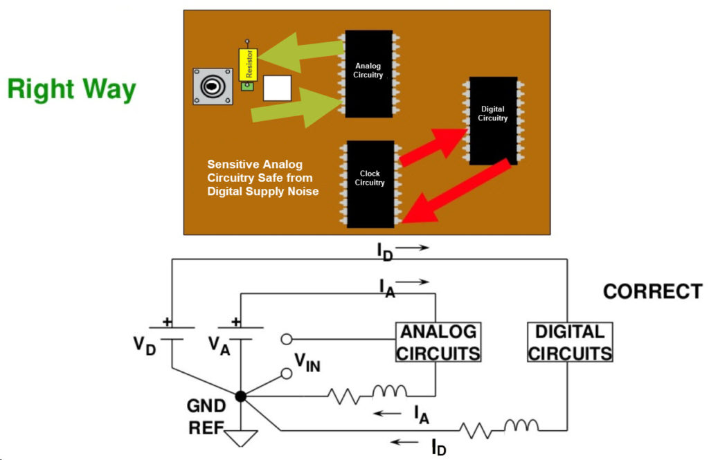
Know where signal and return currents will flow on the PCB for your high frequency and low-frequency signals. Keep digital signals as far away from analog signals as is feasible. Analog circuits are sensitive to digital signals, including the clock, which can introduce noise in the analog side of your system, so separate them and make sure signal paths, or current flows, do not cross. Figure 1, courtesy Analog Devices, shows an incorrect way to place analog and digital circuits on a PCB.
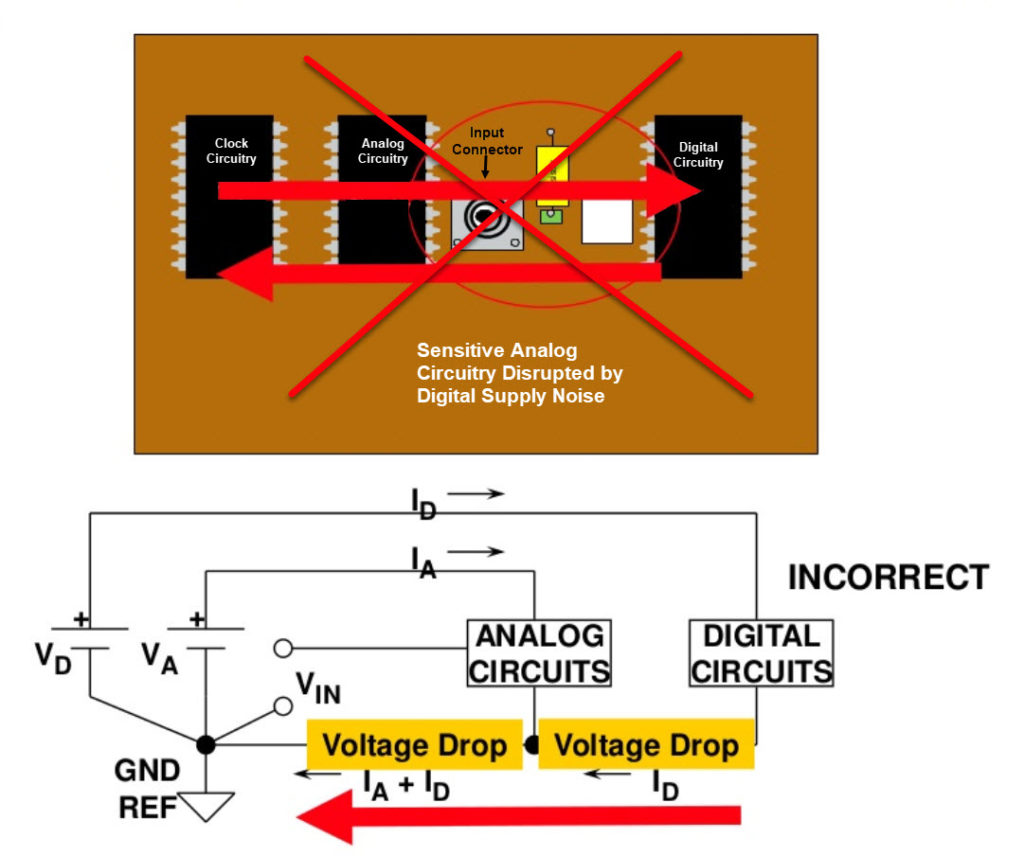
Figure 2 shows analog current flows (green arrows) that do not have to cross over current flows going on between digital circuitry (red arrows).
When you are designing a PCB, the layout and the length of transmission lines of high-speed signals matter. Keep traces as short as possible. Place components physically near the chips that they modify (e.g., pull-up resistors, bypass capacitors). Ground and power planes can provide shielding and if you have a simple PCB, they should be located on opposite sides of the PCB. (Think optimal flow patterns.) Isolate signals using physical separation. Keep parallel traces short as well as traces running on adjacent layers short. Traces that run beside each other or on top of each other (on adjacent layers) can develop parasitic capacitance that results in crosstalk and coupling. If possible, run traces on adjacent layers orthogonal to each other. Remember the electrical relationship to magnetism, and that traces with current running through them create a magnetic field that varies with the signal.
Minimize crosstalk by increasing the distance between traces (or otherwise improve isolation), using guard traces, or by using differential signals to reduce electromagnetic interference. Increasing the distance between traces can be done by increasing board thickness or placing traces as far apart as possible. The smaller the trace or pad area, the lower the equivalent impedance for that area. Traces also have an inductive component, or an approximate trace or strip inductance. Unwanted physical phenomena that can develop, such as capacitance and inductance, can be further investigated in detail by studying the physics behind the relationship between electricity and magnetism. For instance, widening a trace will increase the capacitance of the trace, but it will reduce the inductance of the trace. This is one reason why PCB layout and simulation tools are essential, followed by testing a prototype PCB before attempting production in high volume.
Smaller packages actually do better with high-frequency signals than larger packages, from a PCB layout point-of-view. A compact layout will produce fewer parasitic components. Analog Devices has a “dedicated feedback” on some op amps, designed for making optimal PCB layout of an op amp easier. The dedicated feedback streamlines signal flow and lowers distortion. Analog Devices defines “dedicated feedback” as having placed the feedback pin directly adjacent to the inverting input pin of an op amp. Thus, the only requirement to connect the two pins is a very short trace or resistor rather than routing feedback around or underneath the amplifier.[i]
In addition to keeping trace lengths short, using bypass capacitors is essential. Capacitors need to be placed as close as physically possible to the power supply pins on ICs. Capacitors offer a means to buffer the rise and fall of changing voltage levels and are essential to good performance in high-speed circuits. A ground plane and a power plane are vital to reducing parasitics and noise. For a PCB with multiple layers, at least one layer should be dedicated to a ground plane. Be sure that you have analyzed the return path for current throughout the layout and in all directions. Dedicate as much space as possible to the ground plane, with traces that carry high-speed signals of particular significance in relationship to the ground plane for shielding. For multiple-layer PCBs, use several vias to connect (the same) ground planes together.
Both art and science
As technology has progressed, the frequency of signals, including digital signals, has become blazing fast. Understanding signal propagation has increasingly become a necessity for engineers. To understand why, an article by Dr. Howard Johnson, a high-speed circuit design professor, explains the need to close the gap in understanding between digital design and analog design. Both analog and digital disciplines overlap very noticeably at high speeds, yet have been taught for several decades as if separate worlds (at least to undergraduates). Read Why Johnny Can’t Design a High-Speed Digital System by Dr. Howard Johnson for a long view on some issues that face new engineers.[ii] Designing for a successful PCB layout can be straightforward (for a simple circuit), or an intense science covering several disciplines with a potential for extreme complexity. PCB layout can get complex when driven by product requirements (e.g., size), multiple layers, many and various components, and different types of signals (e.g., high-speed, low voltage, high voltage, digital, analog, etc.) that must successfully co-exist on the same board. Finally, regulations and environmental standards are also part of the PCB design process. Creating well-behaved PCBs is both a science and an art. This article barely scratches the surface, but perhaps it will equip you with an idea of areas that you need to investigate in-depth.
[i] http://www.analog.com/en/analog-dialogue/raqs/raq-issue-65.html
[ii] Find an affordable version of Dr. Johnson’s lecture series at safaribooksonline.com

Thanks for providing information regarding PCB layout guidelines. Really good.
For avoiding crosstalk in numeric high speed designs, take an isolation of 3 times the track width in the most case. In the other cases adapt the ratio depending on the voltage level. For power activities, magnetic and non linear effects needs other pratcices.