Printed circuit boards (PCBs) are essential in modern electronics. Dust and other contaminants are more important to watch out for than ever. As components get smaller, the relative size of contaminants is larger, heat is more of an issue with densely packed circuits on modern ICs, and devices operating at high frequencies (~1 GHz and higher) are more susceptible in many ways.
PCBs are somewhat delicate, so they are usually housed in a cage, case, or chassis. Despite the physical protection that a case provides, processors can run hot and need ventilation to eject heat build-up. Even without a fan, a PCB can still be exposed to dust and liquid pollutants, which can affect performance. Contaminants attract moisture, which can adversely affect the operation of a Microcontroller Unit (MCU). For instance, a typical microcontroller uses voltage levels between 0 and 5v, and if moisture or other conducting contaminants are present between an input pin and a 5v or ground pin, a short circuit is created. An unwanted path for current flow can cause unpredictable behavior, shorten operating lifetime, create a fire hazard, or kill electronics altogether.
Almost every component dissipates power in the form of heat. The heat that builds up beyond specified tolerances can degrade or destroy components. Contaminants can act as insulation on components or block air flow. PCB exposure to liquids, even aerosolized liquids, can cause corrosion on solder joints and circuit traces. Later on, corroded metallic parts can initiate impedance issues or open circuits. Despite the potential for PCB degradation over time, there’s a market for used PCBs. Used or scrap PCBs might be cost-effective for creating small prototype circuits, but they are usually polluted with dust, moisture, or flux and are more often tossed or recycled for metal recovery.
In any case, it’s worthwhile to either protect your PCBs (including computer motherboards) or check on them every few years and clean them if you need them to operate for many years. (You can easily create a filter for a chassis by securing a used dryer sheet over vent slots in a case, as long as the fan is robust enough to tolerate the extra pressure it has to work against. Never, ever use a vacuum cleaner on electronics, however.)
Modern ICs generate more heat than older ICs. Heat increases with greater power consumption, and heat has become more of an issue as integrated chips have packed more circuits in the same amount of space, making ICs more vulnerable to insulating contaminants. Dust can be formed from a variety of organic and inorganic substances such as dirt, hair, plant pollen, clothes, and minerals.[i]
Why do you need flux?
When soldering a PCB, you need flux to “wet” the metal solder to make connections that facilitate metallurgical bonds. Flux also comes in various strengths that dissolve oxides that might have formed on traces, pins, or other metal surfaces that need to solidly connect to create a conductive path. Rosin is a flux material that has been in long use, is made from tree sap, and is fine for use on new components. For repairing electronics or soldering on otherwise dirty PCBs, you can buy mildly activated rosin (RMA) or activated rosin (RA), both of which cut through built-up oxides but leave a residue that needs flux cleaner to end up with a clean PCB that does not attract contaminants. (RA is recommended for heavily oxidized or larger wires.)
Dust
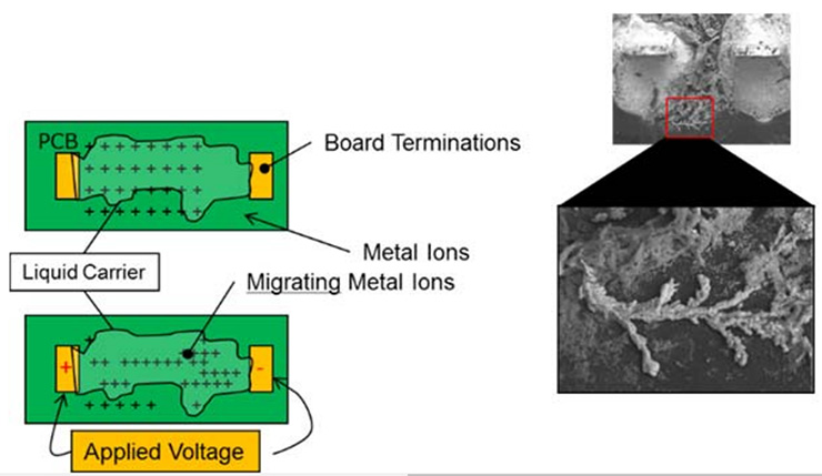
PCBs can suffer from conductivity issues when residual flux from solder joints is left on a PCB. Dust gets attracted to and sticks to flux residues. Electrostatic charge from operating electronics also attracts particles. High-frequency signals, in particular, are affected by the cross-sectional area of a conductive path; therefore performance is affected by the width of conductive traces at high frequencies. Residual flux can be conducive to forming a conductive path, affecting circuit performance. According to the authors of the 2016 white paper Why Clean A No-Clean Flux, “Metal migration is dependent on PCB material composition, board surface roughness, concentration and distribution of residues and environmental conditions.”[ii] Flux residues can lead to electrochemical migration of metal ions and growth of connective metal “dendrites.” No-clean fluxes can leave a light residue that during PCB processing is light enough to evaporate (or outgas) when heat-activated. However, even a no-clean flux residue, if caught under a quad flat-pack IC upon reheat, can try to outgas with nowhere to go and form a bubble under the flat pack IC. Nevertheless, used properly, no-clean flux is reliable and safe.
Three ways to get dirty PCBs
PCBs get dirty enough to affect performance for three reasons: the PCBs are soldered or assembled in an unclean environment, residues are left on the boards after assembly, or finished PCBs are insufficiently protected from the environment during storage or operation.
Assembly in a clean environment is a factor
A clean environment where PCBs are first soldered is a factor in keeping electronics clean and working reliably for a long time. In a dirty environment, dust, particles, or other contaminants can stick to PCBs or get trapped in the solder and keep solid connections from forming, causing conductivity issues later. It is recommended to use soldering gloves, as sweaty fingers can affect PCB just as moisture does.
Please see Why Clean PCBs Matter, Part II for more on this topic.
References:
[i] http://content.time.com/time/health/article/0,8599,1966870,00.html
[ii] https://www.kester.com/LinkClick.aspx?fileticket=Xoh4bQ7bYkc%3D&portalid=0
Nice information can you please also tell me that What is the process and significance of PCB Assembly?