By Brian Hendren, Tektronix
As semiconductor manufacturers start to reach the potential physical limits of shrinking process nodes, chip packaging is emerging to improve performance. Flip chip assembly remains the most popular method for interconnecting dies, but new advancements in silicon interposers are enabling 2.5D packaging architectures and, in turn, making 3D packaging possible.
To help you learn more about the future of chip packaging, I answered a few questions about this emerging field.
Can you explain what 3D packaging entails?
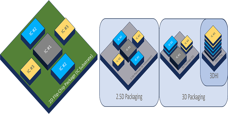
Certainly. 3D packaging involves vertically stacking multiple semiconductors dies (or chiplets), creating a three-dimensional packaging architecture. This approach enables closer integration of different components within a single package.
It is also worth noting that 3D Heterogeneous Integration (3DHI) is a sub-category of 3D packaging. The “heterogeneous” aspect implies that these dies may serve diverse functions and could come from various fabrication processes or vendors.
How is that different from previous forms of packaging?
The key difference lies in the vertical stacking and bonding of components. Traditional packaging methods involve placing chips side by side on a flat surface, limiting the amount of integration. In 3D packaging, components are stacked on top of each other (Figure 1), reducing the distances between them and offering higher integration density.
What sort of benefits does 3D packaging bring?
As electronic devices become more portable, the capacity to make electronics smaller, lighter, and more energy efficient plays a crucial role in shaping the future of technology, especially in consumer, aerospace, and medical devices. So, for the sake of this conversation, let’s focus on size, weight, and power (SWaP).
Size reduction
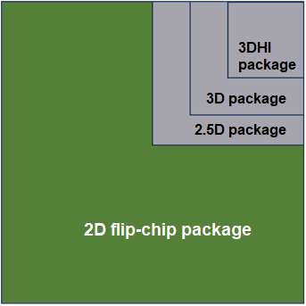
One of the most pronounced benefits of 3D packaging is its size efficiency. Vertically stacking semiconductor components within a single package dramatically reduces the package’s physical footprint. This smaller size is particularly valuable in applications where space is at a premium, such as mobile devices, aerospace systems, and wearable technology. As electronic devices continue to shrink in size, 3D packaging enables the creation of smaller, more compact products (Figure 2) without compromising performance.
Weight Reduction
3D packaging contributes to weight reduction in electronic systems. The compact and densely integrated design achieved through vertical stacking leads to a decrease in the overall weight. This is of paramount importance in sectors such as aerospace, where every gram counts. Lighter electronics can translate to more fuel-efficient aircraft and extended mission capabilities for unmanned aerial vehicles. Weight is also critical in the automotive industry.
Power Efficiency
3D packaging has a twofold impact in terms of power efficiency. Firstly, the vertical stacking of components often results in shorter interconnection lengths. Reduced data travel distances lead to lower signal losses and reduced power consumption. Secondly, the reduction in off-chip communication further enhances power efficiency. With components closely integrated within the 3D package, there’s less need for energy-intensive data transmission between chips, resulting in overall energy savings.
What are the challenges that gate 3D packaging adoption?
3D packaging is in its early stages, so there are several critical challenges before widespread implementation can occur, specifically for deployment in harsh environments. Addressing factors like design for manufacturing (DFM), design for test (DFT), and design for reliability (DFR) will be critical to ensure the success and longevity of 3D-integrated systems.
Here are some examples:
Design for Manufacturing (DFM)
As 3D packaging technologies mature, ensuring efficient and cost-effective manufacturing processes becomes paramount. DFM principles need to be integrated into the design phase to minimize manufacturing complexities and costs. Designers must consider factors like material choices, process compatibility, and yield optimization.
Design for Test (DFT)
Thorough testing of 3D-integrated systems poses unique challenges due to their vertically stacked nature. Designing for testability is critical to developing test strategies that can comprehensively evaluate the functionality and reliability of all components within the 3D package. DFT methodologies need to address accessibility and coverage concerns in the stacked configuration.
Design for Reliability (DFR)
3D packaging introduces new reliability considerations concerning thermal management, stress, and interconnect reliability. Designers must incorporate DFR principles to ensure that the vertically stacked components can withstand environmental stresses, maintain signal integrity, and have a long operational lifespan.
Are there any reasons to be optimistic about the near future of 3D packaging?
I recently attended the Electronics Resurgence Initiative (ERI) 2.0 Summit in Seattle, sponsored by DARPA’s Microsystems Technology Office (MTO). The summit was nothing short of inspiring. It’s evident that we are experiencing global microelectronics competition. DARPA is playing a pivotal role in uniting industry experts, academics, and government stakeholders with a common goal of establishing the United States as the foremost technology leader by creating a national capability for 3DHI manufacturing.
The second reason for excitement is that any push to advance 3D manufacturing capabilities onshore will directly benefit both 2D and 2.5D offerings. As the semiconductor industry focuses on reshoring manufacturing processes and reducing reliance on offshore production, it creates opportunities for strengthening the entire microelectronics ecosystem.
This reinvigoration of domestic manufacturing enhances supply chain resilience and fosters innovation in 2D and 2.5D technologies. With shared resources, research, and infrastructure, advancements made in 3D manufacturing techniques can be leveraged to refine and optimize traditional 2D processes, resulting in more efficient, cost-effective, and sustainable microelectronics solutions. This synergy between 3D, 2D, and 2.5D technologies promises a brighter, more competitive future for the entire industry.


Leave a Reply