MCU low-power features such as built-in energy harvesting help optimize applications where long battery life is important.
Masamitsu Muratani, Renesas
The spectacular growth of the Internet of Things (IoT) is driving the need for devices that are smarter, faster, and can last for long periods on small and inexpensive batteries. To meet such requirements, Renesas has developed a new, ultra-efficient microcontroller (MCU) power management architecture. This architecture is based on Silicon on Thin Buried oxide (SOTB) process technology with the widely used Cortex M series CPU cores at its heart.
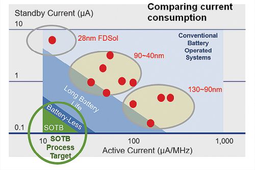
The Silicon on Thin Buried Oxide (SOTB) process is proprietary transistor technology from Renesas based on SOI (Silicon on Insulator) wafers. The benefit of SOTB is it can greatly reduce both active and standby current, which are normally traded off against each other. SOTB has the low-leakage benefits of larger geometries, with the high-performance and low active current benefits of smaller silicon geometries.
In SOTB chips, a thin insulating oxide film (BOX, buried oxide) is deposited on top of the base silicon substrate. Next, a thin silicon layer with no impurities is deposited on top of the BOX insulator layer to form a dopantless channel transistor under the gate, a structure that reduces threshold voltage variance, and thus enables a low operating voltage.
The net effect of the BOX insulating layer and the dopantless channel is high performance, low-voltage operation with both low leakage current and low operational current. To further optimize performance while reducing leakage during standby, a bias voltage may be applied to the base silicon substrate beneath the BOX insulator layer. (As an aside, SOC designers can mix the use of SOTB and standard CMOS bulk transistors as needed to optimize performance, efficiency, and adapt to existing IP designs. Examples of bulk transistor use can be found in I/O ports, charge pumps, and specific analog functions.)
Estimating power consumption
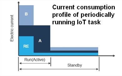
The typical way of computing the power consumption of a system is to first decompose the operation of the system for each task and model the operation time and electrical current each task requires. Additionally, the power assessment process requires defining the cycle time of each task, that is the standby time paired with the operation time.
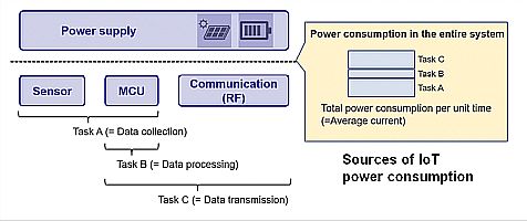
 For IoT devices, three tasks typically define most operations: sensing, data processing, and communication processing. The power consumption of the entire system can be thought of as the sum of the power consumption of these tasks.
It’s evident that the ratio of the active and standby mode times is an important parameter. Important, too, is the magnitude of the electric current in the active and standby modes: The total power consumption of a task is expressed by the area of its current profile. Dividing the total profile area by time yields the average current. A design that reduces the area of the electric current profile is also a design that minimizes power consumption.
The SOTB process technology greatly reduces both active and static power consumption. The digital functions of the device–such as the SRAM, CPU, and peripheral functions–are supplied with a regulated internal voltage and are implemented by transistors based on SOTB technology.
The RE MCU family, based on SOTB process technology, draws low current in both active and standby modes. RE devices having 256 KB flash draw 25 µA/MHz when in active mode (12 µA/MHz with an external dc/dc converter) and a standby current of 0.4 µA (with SRAM retention), 380 nA with a real-time clock only. The RE family can also operate at high speed at a low voltage. Use of multiple power modes lets the MCUs optimize their power consumption for any specific operating condition, making it possible to suppress dynamic current while operating at up to 64 MHz and to reduce leakage current during 32.768-kHz operation and in the standby modes. Developers can design the operating mode transition to suit the application. The key factor should be the duration of the CPU in active mode and active time compared to the standby time.
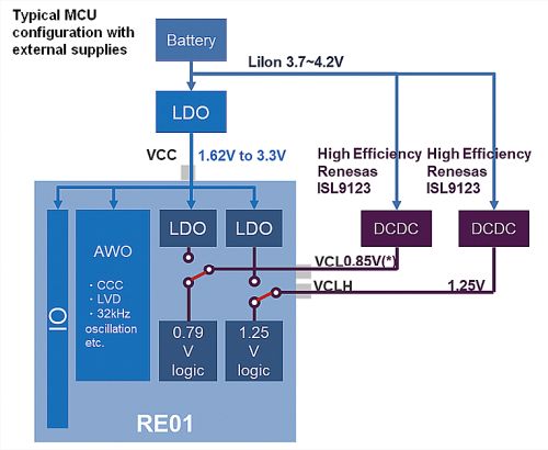
In addition to using power from the built-in power management unit, the RE family has a mechanism to supply power directly to the MCU. This mechanism makes it possible to efficiently convert the main power supply to the required voltage for powering the MCU. The result is better power efficiency for the entire system.
Typical applications combine several devices such as sensors, MCUs and communication modules, each requiring an appropriate power supply voltage. The conversion efficiency involved in generating each voltage factors into the power consumption for the total system.
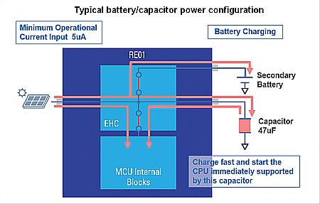
In the interest of IoT battery life, the RE family supports energy harvesting power supplies. This power supply system temporarily stores harvested energy in a capacitor to maintain the MCU operation. Moreover, use of a supercapacitor or a secondary battery in addition to the capacitor can help maintain the system when the supply current from the capacitor alone is insufficient. With a starting current of only 5 µA, the MCU system can operate from an energy harvesting supply having a small current capacity.


Leave a Reply