Representing Micron’s fifth generation of 3D NAND and second-generation replacement-gate architecture, the world’s first 176-layer NAND flash memor features approximately 30 percent smaller die size than best-in-class competitive offerings. Micron’s 176-layer NAND’s compact design is well-suited for small-form-factor applications in spanning data center, intelligent edge, and mobile devices and serves as an essential building block in technologists’ toolboxes across a broad array of sectors, including mobile storage, autonomous systems, in-vehicle infotainment, and client and data center solid-state drives (SSDs).
 The improved quality of service (QoS), a critical design criterion for data center SSDs, accelerates data-intensive environments and workloads such as data lakes, artificial intelligence (AI) engines, and big data analytics. For 5G smartphones, the enhanced QoS can enable faster launching and switching across multiple apps, creating a more seamless and responsive mobile experience and enabling true multitasking and full use of 5G’s low-latency network.
Micron’s fifth generation of 3D NAND also features a maximum data transfer rate at 1,600 megatransfers per second (MT/s) on the Open NAND Flash Interface (ONFI) bus, a 33% improvement. The increased ONFI speed leads to faster system bootup and application performance. In automotive applications, this speed will power near instant-on response times for in-vehicle systems as soon as engines are turned on, enhancing the user experience.
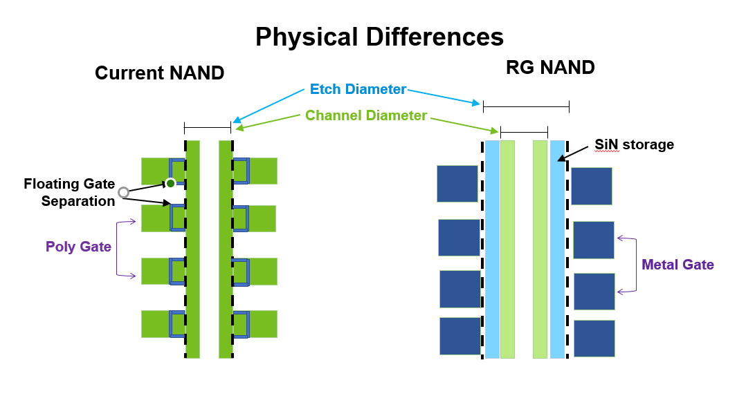
With the slowing of Moore’s Law, Micron’s innovation in 3D NAND is critical to ensuring that the industry can keep pace with growing data requirements. To achieve this milestone, Micron has uniquely combined its stacked replacement-gate architecture, novel charge-trap and CMOS- under-array (CuA) techniques. Micron’s team of 3D NAND experts achieved rapid advancements with the company’s proprietary CuA technique, which constructs the multilayered stack over the chip’s logic — packing more memory into a tighter space and substantially shrinking the 176-layer NAND’s die size, yielding more gigabytes per wafer.
In tandem, Micron has improved scalability and performance for future NAND generations by transitioning its NAND cell technology from legacy floating gate to charge-trap. This charge-trap technology is combined with Micron’s replacement-gate architecture, which uses highly conductive metal wordlines6 instead of a silicon layer to achieve unparalleled 3D NAND performance. Micron’s adoption of this technology will also enable the company to drive aggressive, industry-leading cost reductions.
Applying these advanced techniques, Micron has increased endurance, which is particularly beneficial in write-intensive use cases — from black boxes in aerospace to video surveillance recording. In mobile storage, 176-layer NAND’s replacement-gate architecture results in 15 percent faster mixed workload performance to power ultra-fast edge computing, enhanced AI inference, and graphic-rich, real-time multiplayer gaming.
The 3D NAND is in volume production in Micron’s Singapore fab and now shipping to customers, including through its Crucial consumer SSD product lines. The company will introduce additional new products based on this technology during calendar 2021.


Leave a Reply