The transition from general-purpose computing to AI-specific hardware is driven by the specific computational and energy requirements of deep learning models. As these models scale to trillions of parameters, traditional architectures face the memory wall, where the energy required for data movement between memory and processing units significantly exceeds the energy consumed by the computation itself.
This article outlines the design strategies currently used to address these bottlenecks, ranging from data center systolic arrays to power-constrained edge accelerators.
Q: Why are standard CPU and GPU architectures insufficient for AI workloads?
A: Central processing units (CPUs) are restricted by narrow vector processing units and complex cache hierarchies designed for general-purpose tasks. These features introduce latency in high-concurrency AI operations. While graphics processing units (GPUs) provide higher parallelism, their reliance on the Von Neumann model results in significant power consumption and memory bandwidth limitations.
To address these issues, hardware architects are adopting a multi-layered design approach that spans materials, circuits, architectures, and packaging, as illustrated in Figure 1.
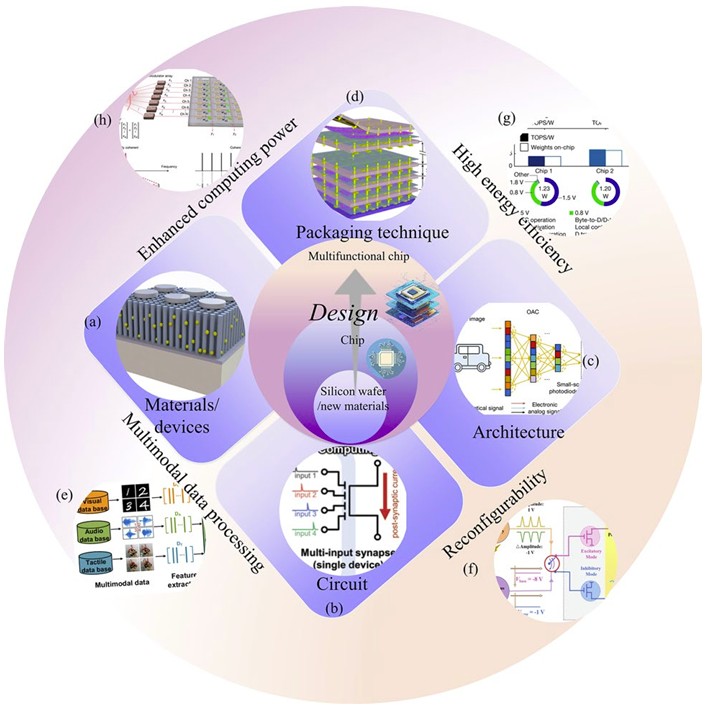
Design efforts generally prioritize four technical pillars, as deconstructed in the multi-layered philosophy shown in Figure 1.
- Computing throughput: Implementing paradigms such as photonic computing or massive parallelization to increase operations per second.
- Energy efficiency: Using Compute-in-Memory (CIM) and non-volatile memory technologies like ReRAM or PCM to reduce the energy cost of data movement.
- Architectural reconfigurability: Designing hardware that can be optimized for different neural network topologies and evolving algorithms.
- Multimodal data integration: Utilizing 3D monolithic integration to combine different processing units, enabling the simultaneous handling of visual, auditory, and textual data with low latency.
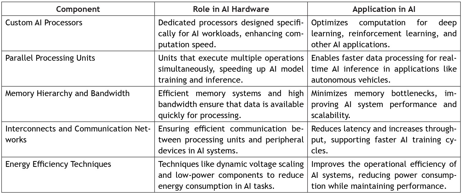
Q: What architectural components are essential for AI hardware acceleration?
A: The shift toward domain-specific architectures involves several foundational components. These are categorized by their specific roles and applications in Table 1:
- Parallel processing elements: General-purpose control logic is replaced with thousands of small, concurrent elements to maximize throughput for matrix-heavy workloads.
- Memory hierarchy optimization: High-bandwidth interconnects and large on-chip buffers are used to maintain data availability for compute units, minimizing the need for off-chip DRAM access.
- Efficiency management: Techniques such as dynamic voltage and frequency scaling and reduced-precision arithmetic (e.g., INT8, FP8, or FP4) allow hardware to function within specific thermal envelopes without significant degradation in inference accuracy.
Q: How is high throughput achieved in data center environments?
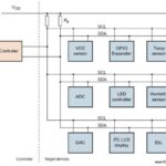
A: Data center inference often relies on application-specific integrated circuits (ASICs), such as Google’s Tensor Processing Unit. The internal data pathways and control interfaces of this architecture are detailed in the block diagram in Figure 2.
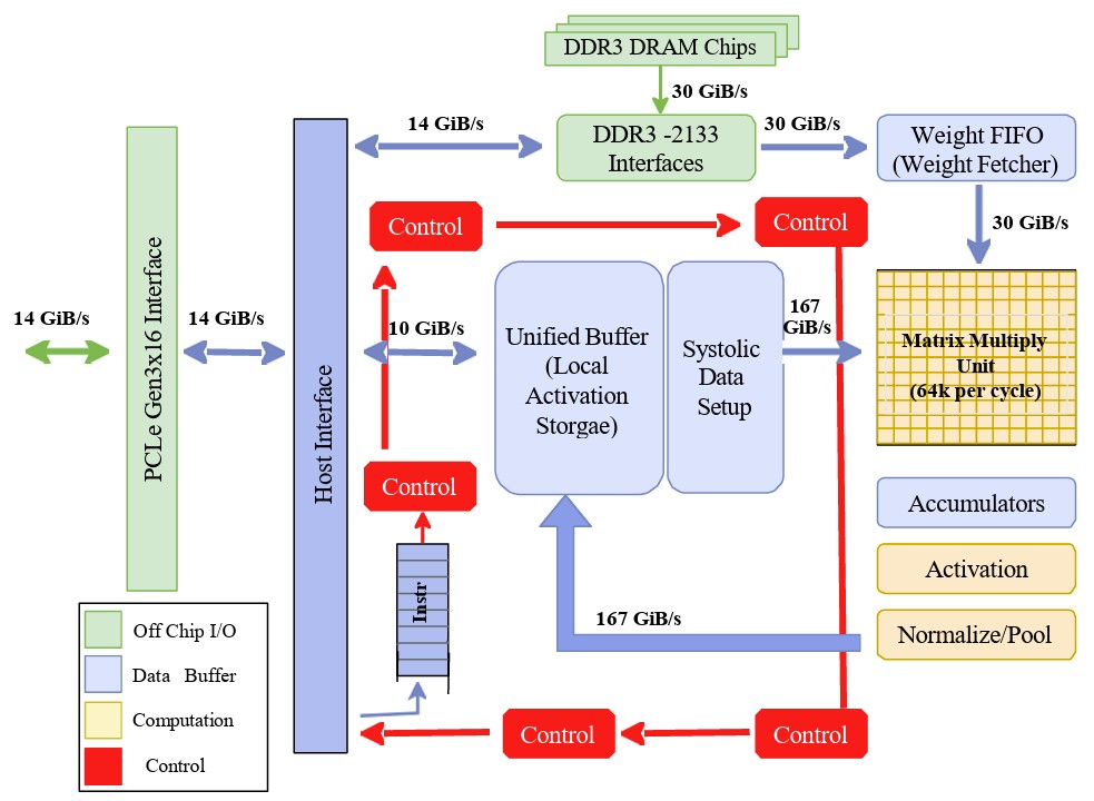
The Matrix Multiply Unit in cloud-scale ASICs utilizes a systolic data flow. In this architecture, data is moved through a grid of arithmetic logic units in a rhythmic pattern. Intermediate results are passed directly between ALUs before being written back to memory.
This design maximizes data reuse and allows the processor to perform tens of thousands of operations per cycle, which is necessary for large-scale Matrix-Vector Multiplications.
Q: How do edge accelerators differ from cloud-based systems in terms of power management?
A: Edge acceleration must operate within much stricter power constraints, often below 25 mW. This requires Algorithm-Hardware Co-Design, a strategy where the software and silicon are designed concurrently to optimize resource usage. A primary example is the Navion chip, whose integrated frontend and backend components are shown in Figure 3.
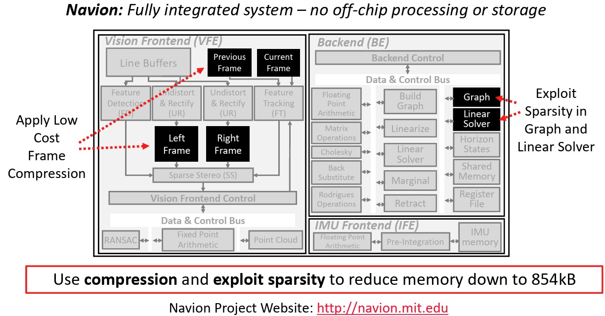
To operate without off-chip DRAM, engineers use several specific strategies highlighted in the Navion architecture in Figure 3:
- Hardware-level data compression: Visual data is compressed at the point of capture to reduce the memory footprint required for storage.
- Sparsity exploitation: To minimize the on-chip memory footprint and reduce processing cycles, the hardware is specifically designed to exploit the natural sparsity found within the backend pose graph and linear solver during Visual-Inertial Odometry computations.
- Frontend coupling: The Vision Frontend and the Inertial Measurement Unit Frontend are tightly integrated to share memory, reducing the required on-chip storage to approximately 854 kB.
Summary
The advancement of AI hardware design is fundamentally a response to the memory wall inherent in Von Neumann architectures. By adopting a multi-layered design philosophy, engineers can optimize performance across materials, circuits, and packaging. In the cloud, this results in high-throughput ASICs utilizing systolic arrays for massive parallel matrix operations.
At the edge, microscopic power budgets necessitate tight algorithm-hardware co-design, utilizing frame compression and sparsity exploitation to maintain functional accuracy without off-chip memory. Ultimately, the future of the field lies in orchestrated heterogeneity and the shift toward CIM to eliminate data movement bottlenecks entirely.
References
Efficient Computing for AI and Robotics: From Hardware Accelerators to Algorithm Design, Massachusetts Institute of Technology
AI Hardware Accelerators: Architectures and Implementation Strategies, Journal of Integrated VLSI
Advanced Design for High-Performance and AI Chips, Springer Nature
Hardware Accelerators for Artificial Intelligence, Arxiv
EEWorld Online related content
How can neuromorphic devices be harnessed in edge AI computing?
What’s the difference between GPUs and TPUs for AI processing?
Accelerating high-performance AI workloads with photonic chips
What is ‘compute-in-memory’ and why is it important for AI?
Kneron AI processors for IoT consume less than 5 mW
What are the different types of AI accelerators?
The three approaches to AI design


Leave a Reply